Jitter control circuit within chip and associated jitter control method

A technology for controlling circuits and chips, which is applied in automatic control of power, control/regulation systems, and measurement of electricity, etc., and can solve problems such as supply voltage noise, severe jitter clocks of clock generators, etc.

Active Publication Date: 2016-12-21
MEDIATEK INC
View PDF5 Cites 1 Cited by
  • Summary
  • Abstract
  • Description
  • Claims
  • Application Information

AI Technical Summary

Problems solved by technology

In addition, since the chip also includes multiple drivers, the driver will draw (sink) current from the power distribution network (PDN), and the current generated by the driver and the impedance of the power distribution network (PDN) are on the power distribution network (PDN) supply voltage noise
This supply voltage noise can cause the on-chip clock generator to generate a clock with serious jitter

Method used


Image

  • Jitter control circuit within chip and associated jitter control method
  • Jitter control circuit within chip and associated jitter control method
  • Jitter control circuit within chip and associated jitter control method

Examples


Embodiment Construction

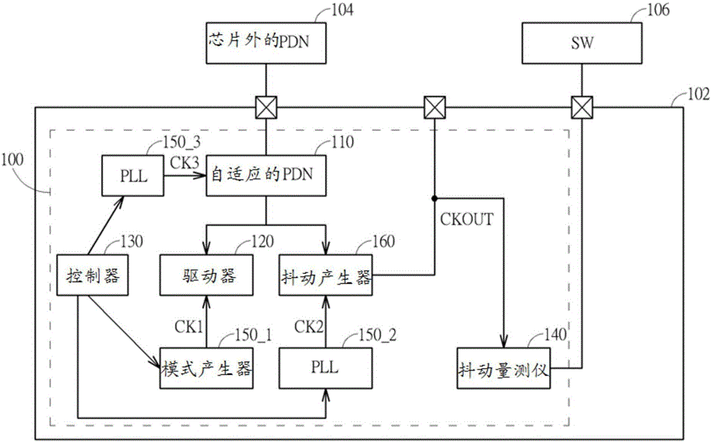
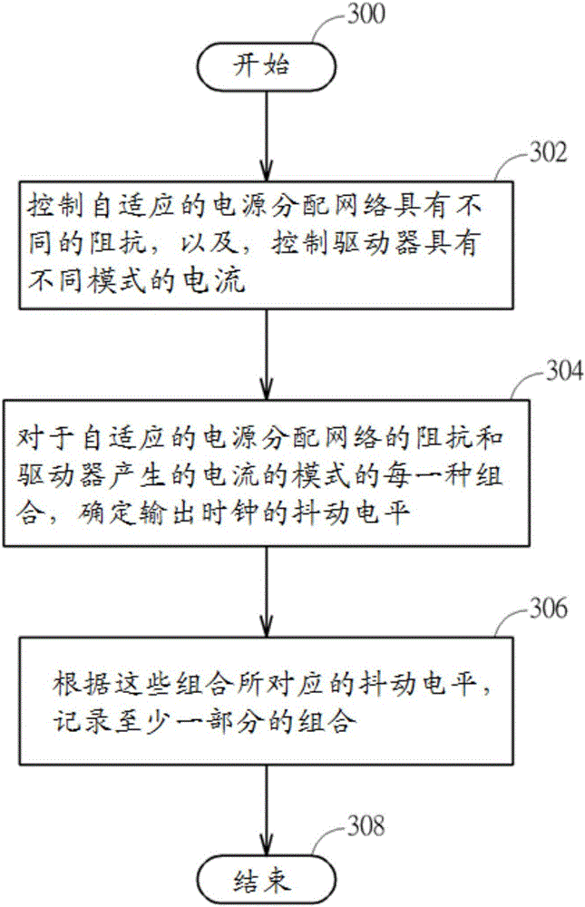
[0013] The following descriptions are preferred embodiments of the present invention, and these preferred embodiments are only used to illustrate the technical features of the present invention, rather than to limit the scope of the present invention. Certain terms are used throughout the specification and claims to refer to particular elements. Those skilled in the art should understand that the manufacturer may use different terms to refer to the same component. Therefore, this description and the claims do not use the difference in name as a way to distinguish components, but the function of the components. difference as a basis for distinction. The terms "element", "system" and "apparatus" used in the present invention may be a computer-related entity, where the computer may be hardware, software, or a combination of hardware and software. The terms "comprising" and "including" mentioned in the following description and claims are open terms, so they should be interpreted...


PUM


Abstract

The invention provides a jitter control circuit within a chip. The jitter control circuit comprises an adaptive PDN, a current generator and a jitter generator. The adaptive PDN is capable of being controlled/modulated to provide difference impedances. The current generator is coupled to the adaptive PDN, and is arranged for receiving a supply voltage provided by the adaptive PDN and generating currents with different patterns. The jitter generator is coupled to the adaptive PDN, and is arranged for generating a plurality of jitters corresponding to the currents with different patterns, respectively, according to the supply voltage provided by the adaptive PDN. The invention further provides a jitter control method. The impedance of the PDN in the chip is adjustable, so that jitter of a signal can be effectively controlled.

Description

technical field [0001] The present invention relates to a technical proposal on jitter control, and more particularly, to a jitter control circuit and a jitter control method located in a chip. Background technique [0002] For a chip powered by an external supply voltage, the external supply voltage is input to the chip through a power delivery network (PDN), which includes many connections, such as a printed circuit board , PCB) wiring, substrate traces, bonding wires, input / output pads and internal metal layers, etc. A power distribution network (PDN) can be modeled as an RLC circuit including resistors, inductors and capacitors, and the impedance of the power distribution network (PDN) varies with frequency on the power distribution network. In addition, since the chip also includes multiple drivers, the driver will draw (sink) current from the power distribution network (PDN), and the current generated by the driver and the impedance of the power distribution network (...

Claims


Application Information

Patent Timeline
Patent Type & Authority Applications(China)
IPC IPC(8): H02M3/00H02M3/155H02M1/00
CPCH02M3/00H02M3/155H02M1/0038H02M1/0003G01R31/31709H03L1/00H03L7/00H04L7/0087H04L7/065
Inventor 陈尚斌李胜丰
Owner MEDIATEK INC
Why Eureka
Try Eureka