Multi-band radio frequency power amplifier

A radio frequency power and amplifier technology, applied in the field of multi-band radio frequency power amplifiers, can solve the problems of high device chip area and cost, and achieve the effects of low cost, lower and use cost, and reduced chip area

Active Publication Date: 2016-12-21
SHANGHAI HUAHONG GRACE SEMICON MFG CORP
View PDF5 Cites 8 Cited by
  • Summary
  • Abstract
  • Description
  • Claims
  • Application Information

AI Technical Summary

Problems solved by technology

[0003] figure 1 There are 3 amplifying circuits in the circuit shown. When the frequency of the radio frequency input signal RFIN is different, the corresponding path is selected for amplifying. Therefore, each frequency band needs a complete set of amplifying circuits, which will make the chip area and cost of the device relatively large. high

Method used


Image

  • Multi-band radio frequency power amplifier
  • Multi-band radio frequency power amplifier
  • Multi-band radio frequency power amplifier

Examples


Embodiment Construction

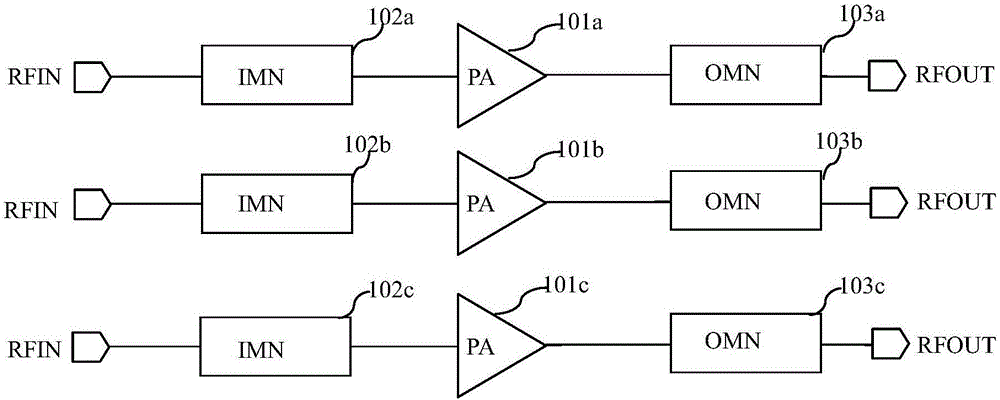
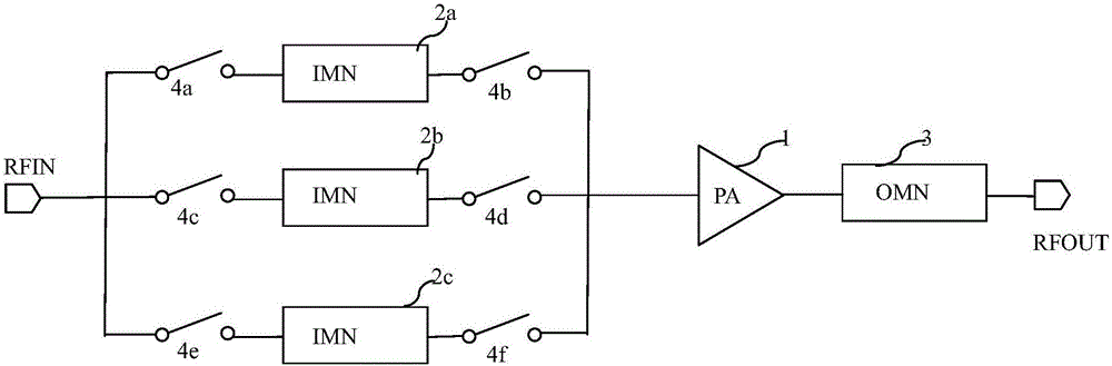
[0033] Such as figure 2 Shown is a circuit diagram of a multi-band radio frequency power amplifier in an embodiment of the present invention; the multi-band radio frequency power amplifier in an embodiment of the present invention includes:

[0034] Multiple input matching network circuits, radio frequency power amplifier circuit 1, and one output matching network 3. In the embodiment of the present invention, the input matching network circuit includes 3 figure 2 The input matching network circuits 2a, 2b, and 2c are selected at frequencies of 900MHz, 1900MHz, and 2400MHz, respectively. in figure 2 The input matching network circuit is represented by IMN, the RF power amplifier circuit is represented by PA, and the output matching network is represented by OMN.

[0035] The amplifier of the radio frequency power amplifying circuit 1 is implemented by the RFSOI process and adopts a stacked MOS tube method to improve withstand voltage and output power.

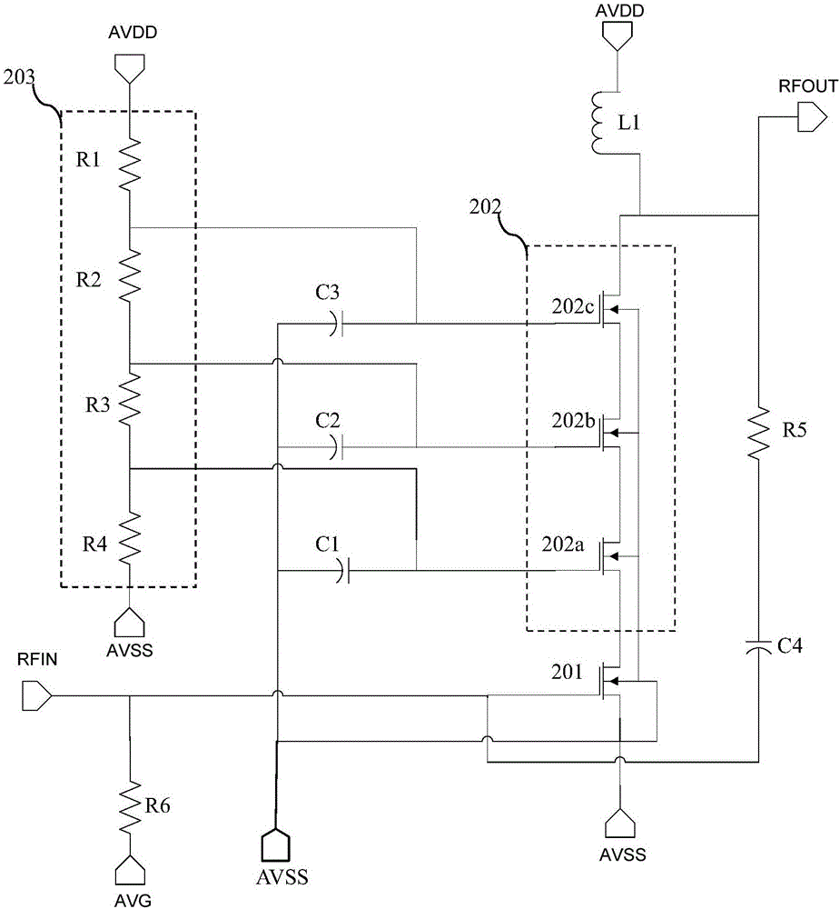
[0036] The input end of ea...


PUM


Abstract

The invention discloses a multi-band radio frequency power amplifier, comprising multiple input matching network circuits, a radio frequency power amplifier circuit and an output matching network. The amplifier of the radio frequency power amplifier circuit is realized by employing an RFSOI technology, and through adoption of a mode of stacking MOS transistors, the withstand voltage and output power are improved. The input end of each input matching network is connected with a radio frequency input signal through a switch. The output end of each input matching circuit is connected with the input end of the radio frequency power amplifier circuit through a switch. Corresponding input matching networks are selected through the switches according to the difference of bands to which the frequency of the radio frequency input signals belong, thereby realizing input of multi-band radio frequency input signals. The output end of the radio frequency power amplifier circuit is connected with the input end of the output matching network. The output end of the output matching circuit outputs radio frequency output signals. According to the power amplifier, the chip area and usage cost can be greatly reduced.

Description

Technical field [0001] The invention relates to a semiconductor integrated circuit, in particular to a multi-band radio frequency power amplifier. Background technique [0002] The RF power amplifier is the main energy-consuming component of the RF front-end. The RF power amplifier works in a certain frequency range, and the output power and efficiency of the RF power amplifier are greatly reduced when the frequency exceeds a certain frequency range. The RF power amplifier often works in different frequency states. In order to adapt to different frequency ranges, existing methods usually need to use two or more radio frequency power amplifiers to meet each frequency range. Such as figure 1 Shown is the circuit diagram of an existing multi-band RF power amplifier, figure 1 The CCP has adopted three radio frequency power amplifier circuits (PA), as shown in the marks 101a, 101b, and 101c. Input matching network circuits (IMN) are connected to the input ends of the radio frequency ...

Claims


Application Information

Patent Timeline
IPC IPC(8): H03F3/193H03F3/21H03F3/24
CPCH03F3/193H03F3/21H03F3/245
Inventor 刘国军
Owner SHANGHAI HUAHONG GRACE SEMICON MFG CORP
Why Eureka
Try Eureka