

A large-area horizontal depletion neutron detector and its preparation method
A neutron detector, depletion type technology, used in semiconductor devices, final product manufacturing, sustainable manufacturing/processing, etc. Poor and other problems, to achieve the effect of reducing costs
- Summary
- Abstract
- Description
- Claims
- Application Information
AI Technical Summary
Problems solved by technology
Method used
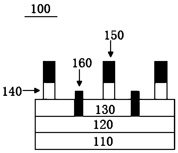
Image


Examples
Embodiment Construction
[0022] Exemplary embodiments of the present invention will be described in detail below with reference to the accompanying drawings.
[0023] Exemplary embodiments of the present invention will be described in detail below in conjunction with the accompanying drawings, however, the accompanying drawings only schematically illustrate specific examples of the present invention and are not limiting. However, it should be understood by those skilled in the art that various modifications and variations can be made thereto without departing from the scope of protection defined by the claims of the present invention.
[0024] CuInSe 2 It is an important chalcogenide semiconductor photoelectric thin film, which can be combined with compounds such as CdS to prepare polycrystalline thin film solar cells. can be tuned by CuInSe 2 The particle size, chemical composition and stoichiometric ratio of the material are used to adjust the band gap width, that is, the range of particle absorpt...
PUM
 Abstract
Description
Claims
Application Information