Processing method of microstructure array

A technology of microstructure arrays and processing methods, which is applied in the direction of metal processing equipment, electrochemical processing equipment, manufacturing tools, etc., can solve the problems of narrow application range of masks and complicated mask preparation, and achieve easy implementation and simple mask preparation Effect

Inactive Publication Date: 2017-01-04
HENAN POLYTECHNIC UNIV
View PDF6 Cites 16 Cited by
  • Summary
  • Abstract
  • Description
  • Claims
  • Application Information

AI Technical Summary

Problems solved by technology

[0005] The purpose of the present invention is to overcome the shortcomings of complex mask preparation and narrow mask application range in the existing mask electrolytic processing, and propose a processing method for microstructure arrays, using atomized emulsified wax droplets as a mask, which can realize Fabrication of large-area microstructure arrays

Method used


Image

  • Processing method of microstructure array
  • Processing method of microstructure array
  • Processing method of microstructure array

Examples


Embodiment Construction

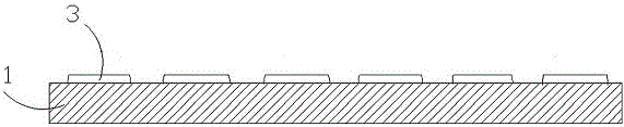
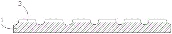
[0028] Combine below figure 1 , figure 2 , image 3 with Figure 4 The present invention is specifically illustrated for further description.

[0029] A processing method of a microstructure array of the present embodiment comprises the following steps:

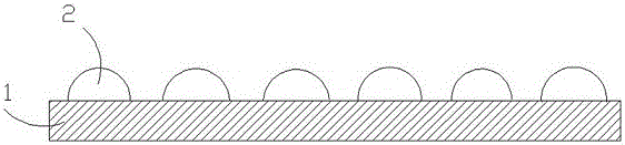
[0030] (1) Take a certain amount of emulsified wax, atomize and evenly spray the emulsified wax on the surface 1 of the workpiece to be processed with atomization equipment, so that the atomized emulsified wax droplets 2 are discrete and evenly attached to the surface 1 of the workpiece to be processed superior.

[0031] The surface of the workpiece to be processed should be polished, degreased and derusted. Preferably, the material of the workpiece to be processed is a conductive material with good electrolytic machining performance, such as nickel, copper or stainless steel. The workpiece to be processed used in this example is a stainless steel sheet.

[0032] Preferably, the emulsifying wax adopts polypropylene wa...


PUM

PropertyMeasurementUnit
melting pointaaaaaaaaaa

Abstract

The invention discloses a processing method of a microstructure array. The processing method includes the following steps that 1, a certain amount of emulsifying wax is taken, and the emulsifying wax is atomized and uniformly sprayed to the surface of a workpiece to be processed through atomizing equipment so that atomized emulsifying wax droplets can be dispersed and uniformly attached to the surface of the workpiece to be processed; 2, the emulsifying wax droplets on the surface of the workpiece to be processed are solidified to form a dispersed wax film uniformly applied to the surface of the workpiece to be processed; 3, the workpiece to be processed with the dispersed wax film attached is put into an electrolytic cell, an electrolyte is introduced, electrolytic processing is carried out with the workpiece to be processed as the anode and the wax film as the mask, and the zone not covered with the wax film is etched to obtain microstructures; 4, after the microstructures meet the processing requirement, the workpiece is taken out, cleaned and dried; 5, the wax film on the surface of the workpiece is removed, and the needed microstructure array is obtained. The processing method is simple in technology and low in cost, and the large-area microstructure array can be processed at a time.

Description

technical field [0001] The invention relates to a processing method of a microstructure array, which belongs to the field of electrochemical processing. Background technique [0002] In recent years, with the increasing requirements for the surface properties of objects, especially the surface properties of important friction pairs, the surface microstructure has developed rapidly due to its excellent anti-friction properties. In addition, the formation of micro- and nano-scale microstructures on the solid surface can effectively reduce its surface wettability; the microstructure of the surface of biological implants can enable cells to respond to the micro- and nano-scale surface topology when recognizing the surface features of materials, and produce "Contact-led" phenomenon. [0003] At present, the commonly used microstructure processing methods are: ultra-precision machining technology, EDM, ultrasonic processing, microwave processing, laser processing, electron beam p...

Claims


Application Information

Patent Timeline
Patent Type & Authority Applications(China)
IPC IPC(8): B23H9/00B23H3/00
CPCB23H9/008B23H3/00
Inventor 秦歌王冠周红梅周奎赵西梅李润清明平美
Owner HENAN POLYTECHNIC UNIV
Why Eureka
Try Eureka