Unlock instant, AI-driven research and patent intelligence for your innovation.

Memory device and manufacturing method thereof

A manufacturing method and memory technology, applied in semiconductor/solid-state device manufacturing, transistors, electrical components, etc., can solve problems such as process difficulty and improvement, and achieve the effect of improving leakage current and bit line coupling interference

Active Publication Date: 2017-01-04
WINBOND ELECTRONICS CORP
View PDF5 Cites 0 Cited by
  • Summary
  • Abstract
  • Description
  • Claims
  • Application Information

AI Technical Summary

Problems solved by technology

However, within a limited unit area, stacked capacitors need to have a considerable capacitance height to ensure sufficient capacitance to store charges. This additional height also increases the difficulty of the process, and there are still many problems to be overcome.

Method used


Image

  • Memory device and manufacturing method thereof
  • Memory device and manufacturing method thereof
  • Memory device and manufacturing method thereof

Examples


Embodiment Construction

[0039] The structure and fabrication of the embodiments of the present invention are described below. Embodiments of the invention provide many suitable inventive concepts that may be broadly implemented in a variety of specific contexts. The specific embodiments disclosed are only used to illustrate how to make and use the invention in a specific way, and are not intended to limit the scope of the invention.

[0040] In addition, repeated reference symbols and / or words may be used in various embodiments of the present invention. These repeated symbols or words are used for the purpose of simplification and clarity, and are not used to limit the relationship between various embodiments and / or the appearance structures.

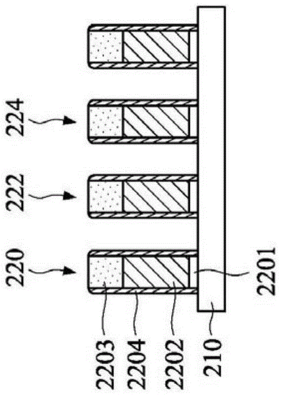
[0041] figure 1 A capacitive terminal contact structure is shown. In a stacked memory device, due to structural stacking and IC design, the capacitor and the capacitor terminal contact structure are often not fully aligned. To help the capacitor connect the...


PUM


Abstract

The invention provides a memory device and a manufacturing method thereof. The memory device comprises a substrate, a plurality of bit lines, a first isolation structure, a second isolation structure, a plurality of bottom contact structures and a plurality of top contact structures, and is characterized in that the plurality of bit lines extend on the substrate in a parallel manner along a first direction; the first isolation structure and the second isolation structure extend on the substrate and the bit line along a second direction; the plurality of bottom contact structures are arranged between the bit lines along the second direction so as to enable the first isolation structures and the second isolation structure to be arranged at two sides of the bottom contact structures in the first direction; and the plurality of top contact structures are arranged on the bottom contact structures, and each top contact structure is provided with a shoulder portion which presses against the top surface of the corresponding first isolation structure.

Description

technical field [0001] The present invention relates to memory devices and methods of fabrication thereof, and more particularly to contact structures and methods of fabrication thereof. Background technique [0002] With the progress of integrated circuit technology, all kinds of electronic components are developing towards high integration, high speed operation and miniaturization. For random dynamic access memories (dynamic random access memories, DRAM), due to the increase in memory capacity and the continuous shrinking of the process, it is necessary to increase the capacitance of each memory cell (memory cell) and prevent short-circuit failure caused by capacitive dumping. In order to meet the development needs of DRAM in the future. [0003] DRAM technology can be mainly divided into two types: trench type and stack type. Among them, due to the low process difficulty, stacked capacitors have become the mainstream of commercial DRAM, and various stacked types have be...

Claims


Application Information

Patent Timeline
IPC IPC(8): H01L27/108H01L21/8242
Inventor 邱威鸣赵元宏
Owner WINBOND ELECTRONICS CORP
Features
  • R&D
  • Intellectual Property
  • Life Sciences
  • Materials
  • Tech Scout
  • Unparalleled Data Quality
  • Higher Quality Content
  • 60% Fewer Hallucinations
Learn More