Array substrate, manufacturing method therefor, and liquid crystal display panel
What is Al technical title?
Al technical title is built by PatSnap Al team. It summarizes the technical point description of the patent document.
A technology of array substrate and manufacturing method, which is applied in semiconductor/solid-state device manufacturing, electrical components, electric solid-state devices, etc., can solve the problems of GOA circuit design difficulties, large area occupied by capacitors, and increased size, so as to reduce the occupation space, achieve narrow frame design, and increase the effect of facing the area
Inactive Publication Date: 2017-01-04
TCL CHINA STAR OPTOELECTRONICS TECH CO LTD
View PDF10 Cites 12 Cited by
Summary
Abstract
Description
Claims
Application Information
AI Technical Summary
This helps you quickly interpret patents by identifying the three key elements:
Problems solved by technology
Method used
Benefits of technology
Problems solved by technology
However, the Boost capacitor usually needs to reach the picofarad (pF) level to make the GOA circuit work effectively. For example, the capacitance area of a 10pF Boost capacitor usually needs to reach 0.1mm 2 , for a higher resolution LCD (Liquid Crystal Display, liquid crystal display) panel, the size of the TFT and Boost capacitor needs to be further increased
In other words, the area occupied by TFT and Boost capacitors is relatively large, which brings great difficulties to the design of narrow-frame, high-resolution GOA circuits
Method used
Image
Click on the blue label to locate the original text in one second.
Reading with bidirectional positioning of images and text.
Examples
Embodiment Construction
[0027] The following will clearly and completely describe the technical solutions in the embodiments of the present invention with reference to the accompanying drawings in the embodiments of the present invention. Obviously, the described embodiments are only part of the embodiments of the present invention, not all of them. Based on the embodiments of the present invention, all other embodiments obtained by persons of ordinary skill in the art without making creative efforts belong to the protection scope of the present invention.
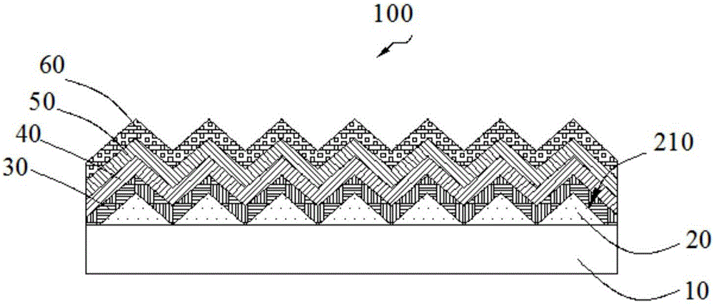
[0028] In addition, the following descriptions of the various embodiments refer to the attached drawings to illustrate specific embodiments in which the present invention can be implemented. The directional terms mentioned in the present invention, for example, "upper", "lower", "front", "rear", "left", "right", "inner", "outer", "side", etc., only is to refer to the direction of the attached drawings. Therefore, the direction terms used are for ...
PUM
Abstract
The invention provides an array substrate, and the array substrate comprises a glass substrate, a photoresist layer, a first metal layer, a dielectric layer, a buffering layer and a second metal layer, wherein the glass substrate, the photoresist layer, the first metal layer, the dielectric layer, the buffering layer and the second metal layer are sequentially stacked. A side, close to the first metal layer, of the photoresist layer is provided with a plurality of bulged structures, and the first metal layer covers the bulged structures. The first metal layer, the dielectric layer, the buffering layer and the second metal layer has the same shape as the bulged structures. According to the invention, the photoresist layer is provided with the bulged structures, thereby enabling the firs metal layer, the dielectric layer, the buffering layer and the second metal layer on the bulged structures to be corrugated, increasing the opposite area of the first and second metal layers, increasing the equivalent capacitance, facilitating the reduction of a space occupied by an equivalent capacitor, and achieving a narrow frame design. A manufacturing method for the array substrate can reduce the space occupied by the equivalent capacitor, and achieves the narrow frame design.
Description
technical field [0001] The invention relates to the technical field of displays, in particular to an array substrate, a manufacturing method thereof, and a liquid crystal display panel. Background technique [0002] In the prior art, usually in the array process stage of the liquid crystal display panel, the gate driver circuit is manufactured on the array substrate by using GOA (Gate Driver OnArray) technology, so as to realize the progressive scan driving of the gate lines. Compared with traditional COF (Chip On Flex / Film, chip-on-film) technology and COG (Chip OnGlass, chip directly bonded to glass) technology, GOA technology can reduce manufacturing costs. The main feature of GOA technology is that it relies on continuous triggering of GOA units. Realize the shift register function, save the bonding area of the gate integrated circuit (Gate IC) and the Fan-out wiring space, and realize the design of the narrow frame. [0003] In GOA circuit design, TFT (Thin Film Tran...
Claims
Application Information
Patent Timeline
Application Date:The date an application was filed.
Publication Date:The date a patent or application was officially published.
First Publication Date:The earliest publication date of a patent with the same application number.
Issue Date:Publication date of the patent grant document.
PCT Entry Date:The Entry date of PCT National Phase.
Estimated Expiry Date:The statutory expiry date of a patent right according to the Patent Law, and it is the longest term of protection that the patent right can achieve without the termination of the patent right due to other reasons(Term extension factor has been taken into account ).
Invalid Date:Actual expiry date is based on effective date or publication date of legal transaction data of invalid patent.