Diode Anode Structures, Vertical Diodes, and Lateral Diodes

An anode structure and diode technology, applied in the direction of semiconductor devices, electrical components, circuits, etc., can solve the problem of increasing the forward turn-on voltage, and achieve the effect of reducing the forward turn-on voltage, improving the efficiency, and solving the forward turn-on voltage.

Active Publication Date: 2019-11-15
GPOWER SEMICON
View PDF5 Cites 0 Cited by
  • Summary
  • Abstract
  • Description
  • Claims
  • Application Information

AI Technical Summary

Problems solved by technology

[0005] In view of this, an embodiment of the present invention provides a diode anode structure, a vertical diode, and a horizontal diode to solve the technical problem of increasing the forward turn-on voltage when reducing the reverse leakage of the Schottky diode in the prior art

Method used


Image

  • Diode Anode Structures, Vertical Diodes, and Lateral Diodes
  • Diode Anode Structures, Vertical Diodes, and Lateral Diodes
  • Diode Anode Structures, Vertical Diodes, and Lateral Diodes

Examples


Embodiment 1

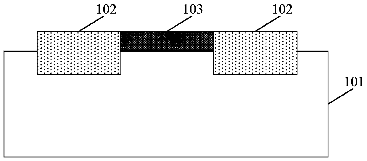
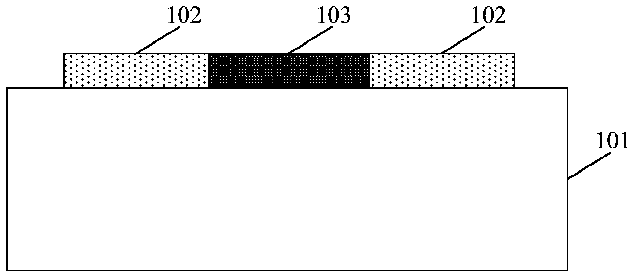
[0046] Figure 1a and Figure 1b Both are schematic cross-sectional structure diagrams of a diode anode structure provided in Embodiment 1 of the present invention. Specifically, the diode anode structure provided in the embodiment of the present invention includes two different types of Schottky metal layers. Such as Figure 1a and Figure 1b As shown, the diode anode structure may include:

[0047] semiconductor layer 101;

[0048] At least two first Schottky metal layers 102 are located on the semiconductor layer 101 and form Schottky contacts with the semiconductor layer 101 to obtain a first Schottky barrier height;

[0049] At least one second Schottky metal layer 103 is located on the semiconductor layer 101 and between the first Schottky metal layers 102 to form a Schottky contact with the semiconductor layer 101 to obtain a second Schottky barrier height.

[0050] Specifically, such as Figure 1a As shown, a groove structure corresponding to the first Schottky meta...

Embodiment 2

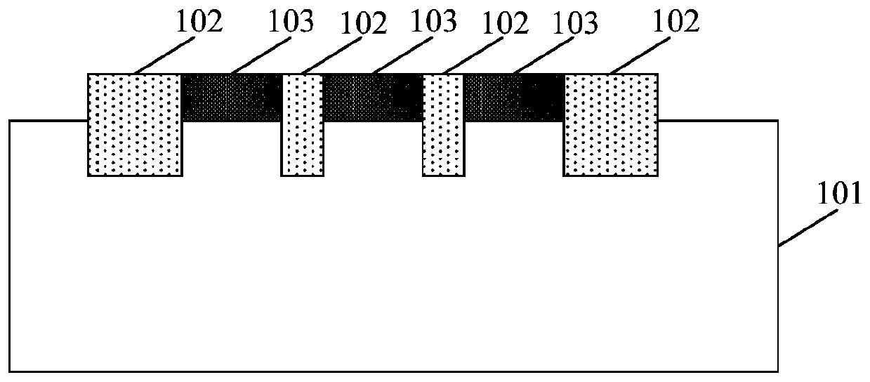
[0059] Figure 2a , Figure 2b , Figure 2c and Figure 2d Both are structural schematic diagrams of a diode anode structure provided in Embodiment 2 of the present invention. This embodiment is based on Embodiment 1 and adjusted on the basis of Embodiment 1. Specifically, the diode anode structure provided by the embodiment of the present invention includes multiple first Schottky metal layers 102 and multiple second Schottky metal layers 103 .

[0060] Such as Figure 2a as shown, Figure 2a The number of first Schottky metal layers 102 located on the semiconductor layer 101 is four, and the number of second Schottky metal layers 103 located on the semiconductor layer 101 and between the first Schottky metal layers 102 The number is three. In practical applications, the number and distance between the first Schottky metal layer 102 and the second Schottky metal layer 103 can be adjusted according to the requirements of forward turn-on current and reverse leakage current...

Embodiment 3

[0065] Figure 3a and Figure 3b Both are schematic cross-sectional structural diagrams of a diode anode structure provided in Embodiment 3 of the present invention. This embodiment is based on the above-mentioned embodiments and is optimized on the basis of the above-mentioned embodiments. Specifically, in the diode anode structure provided by the embodiment of the present invention, a potential barrier adjustment region is formed between the first Schottky metal layer 102 and the semiconductor layer 101 .

[0066] Such as Figure 3a As shown, a potential barrier adjustment region 104 is formed between the first Schottky metal layer 102 and the semiconductor layer 101 , and the potential barrier adjustment region 104 is disposed corresponding to the first Schottky metal layer 102 . Figure 3a In the shown diode anode structure, a groove structure is formed between the semiconductor layer 101 and the first Schottky metal layer 102 , so the barrier adjustment region 104 can b...


PUM


Abstract

The embodiment of the invention discloses a diode anode structure, a vertical diode and a transverse diode, and relates to the technical field of semiconductors. The diode anode structure comprises a semiconductor layer, at least two first Schottky metal layers, and at least one second Schottky metal layer, the two first Schottky metal layers are located on the semiconductor layer and forms Schottky contact with the semiconductor layer to obtain a first Schottky barrier height, and the at least one second Schottky metal layer is located on the semiconductor layer and between the first Schottky metal layers, and forms Schottky contact with the semiconductor layer to obtain a second Schottky barrier height. By employing the above technical scheme, two barrier heights are formed at an anode area with a semiconductor, when the diode is turned off in a reverse manner, the first Schottky barrier height can reduce reverse leakage, when the diode is turned on in a forward manner, the second Schottky barrier height can reduce forward turn-on voltage, and the usage efficiency of the diode can be improved by employing the above diode anode structure.

Description

technical field [0001] The embodiments of the present invention relate to the technical field of semiconductors, and in particular to a diode anode structure, a vertical diode and a horizontal diode. Background technique [0002] In the field of high-voltage switch applications, in order to improve efficiency and reduce losses, diodes are required to have the characteristics of small reverse leakage, large reverse withstand voltage and small forward conduction voltage drop. Power electronic devices based on wide-bandgap semiconductor materials, especially gallium nitride materials, have superior properties. Therefore, Gallium Nitride Schottky diodes have gradually become a research hotspot in recent years. [0003] As we all know, the PN junction diode has a large forward voltage drop, so its conduction loss is large, but its reverse leakage current is small, and its off-state loss is small. Schottky diodes have the characteristics of small forward voltage drop and large r...

Claims


Application Information

Patent Timeline
Patent Type & Authority Patents(China)
IPC IPC(8): H01L29/872H01L29/47
CPCH01L29/475H01L29/872
Inventor 邓光敏裴轶
Owner GPOWER SEMICON
Why Eureka
Try Eureka