Nondestructive cleaning device of graphic wafer capable of improving cleaning uniformity

A cleaning device and non-damaging technology, applied in cleaning methods and utensils, cleaning methods using liquids, electrical components, etc., can solve distance changes, damage to the pattern structure of the wafer surface in local areas, and reduce the removal efficiency of regional particle contaminants, etc. problem, to achieve the effect of uniform energy distribution

Active Publication Date: 2017-01-11
BEIJING SEVENSTAR ELECTRONICS CO LTD
View PDF4 Cites 4 Cited by
  • Summary
  • Abstract
  • Description
  • Claims
  • Application Information

AI Technical Summary

Problems solved by technology

If the ultrasonic / megasonic energy obtained during the cleaning process is too little, the removal efficiency of particle pollutants in this area will be reduced. If the energy obtained is too much, it may cause damage to the pattern structure of the wafer surface in a local area
[0009] However, in the cleaning device disclosed in the above-mentioned Chinese invention patent application, the lower end bottom surfaces of all the quartz rods in the quartz rod array on the bottom surface of the device are flush.
If the bottom surface of the device is not perfectly parallel to the surface of the wafer, the distance between the two will vary greatly with position, resulting in uneven distribution of acoustic energy
For example, when the ultrasonic / megasonic cleaning device covers a fan-shaped area from the center to the edge of the wafer, the distance between the bottom surface of the device at the center of the wafer and the wafer may be small, and as the radius gradually increases, the distance between the bottom surface of the device and the wafer Gradually increasing problems, resulting in uneven distribution of acoustic energy

Method used


Image

  • Nondestructive cleaning device of graphic wafer capable of improving cleaning uniformity
  • Nondestructive cleaning device of graphic wafer capable of improving cleaning uniformity
  • Nondestructive cleaning device of graphic wafer capable of improving cleaning uniformity

Examples


Embodiment Construction

[0052] The specific embodiment of the present invention will be further described in detail below in conjunction with the accompanying drawings.

[0053] It should be noted that, in the following specific embodiments, when describing the embodiments of the present invention in detail, in order to clearly show the structure of the present invention for the convenience of description, the structures in the drawings are not drawn according to the general scale, and are drawn Partial magnification, deformation and simplification are included, therefore, it should be avoided to be interpreted as a limitation of the present invention.

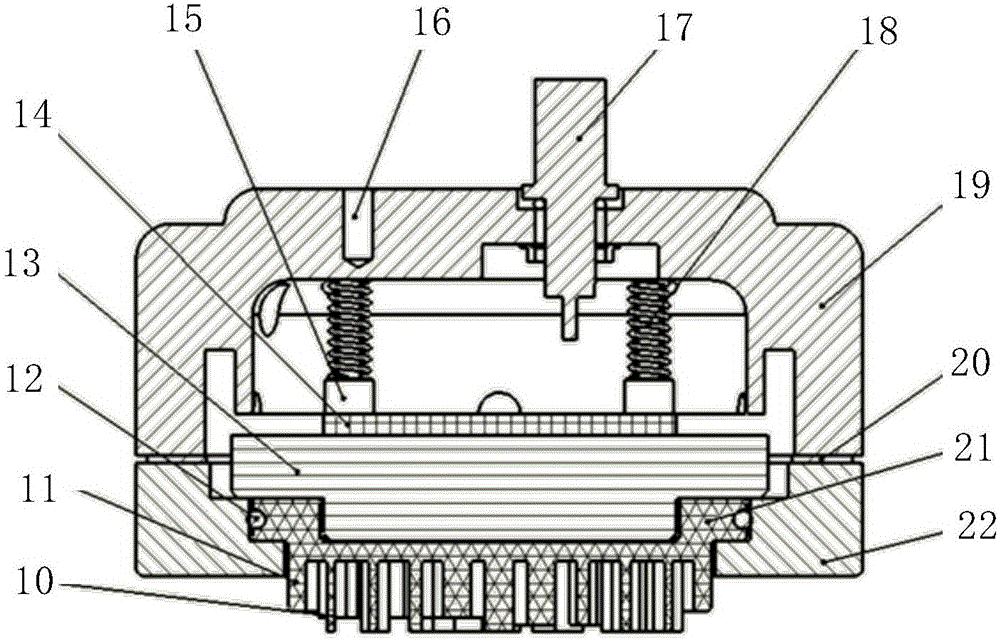
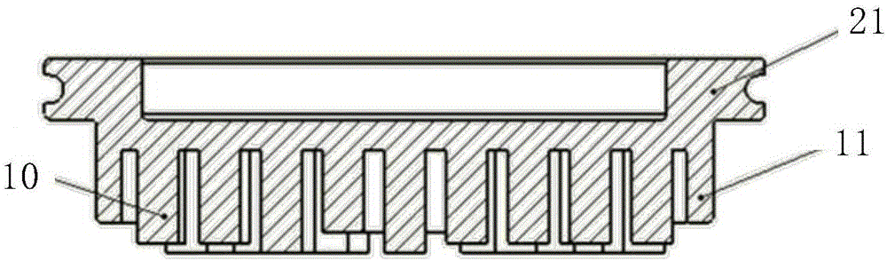
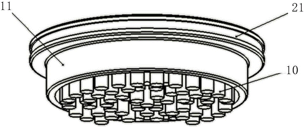
[0054] In the following specific embodiments of the present invention, first please refer to figure 1 , figure 1 It is a structural cross-sectional view of a non-damage cleaning device for patterned wafers that improves cleaning uniformity in an embodiment of the present invention. Such as figure 1 As shown, a non-damage cleaning device for patter...


PUM


Abstract

The invention discloses a nondestructive cleaning device of a graphic wafer capable of improving the cleaning uniformity. An ultrasonic/megasonic generation mechanism and a bottom quartz device which are clung from top to bottom are arranged in a shell seal cavity, wherein the bottom quartz device comprises connected annular quartz microresonator protection ring and quartz microresonator array; the quartz microresonator array comprises a plurality of vertical rodlike quartz structures; the lower end of a groove of the annular quartz microresonator protection ring extends outside from the lower end surface of the shell; the lower end surface of the quartz microresonator array is not higher than that of the groove and the lower end surfaces of the rodlike quartz structures have different heights; and ultrasonic/megasonic energy of which the propagation direction is not vertical to the surface direction of the wafer can be selectively removed through the quartz microresonator array and the ultrasonic/megasonic energy on the surface of the graphic wafer can be uniformly distributed, thereby achieving a uniform and nondestructive cleaning effect in a random region in the overall graphic wafer range within certain cleaning time.

Description

technical field [0001] The invention relates to the field of processing and cleaning equipment for semiconductor integrated circuits, and more particularly relates to a non-damage cleaning device for cleaning pattern wafers and improving cleaning uniformity. Background technique [0002] With the rapid development of semiconductor integrated circuit manufacturing technology, the graphic feature size of integrated circuit chips has entered the deep sub-micron stage, and the feature size of key contaminants (such as particles) that cause failure or damage to ultra-fine circuits on the chip has also changed. greatly reduced. [0003] During the production and processing process of integrated circuits, semiconductor wafers usually go through multiple process steps such as film deposition, etching, and polishing. And these process steps just become the important place that the contamination produces. In order to maintain the clean state of the wafer surface and eliminate the co...

Claims


Application Information

Patent Timeline
Patent Type & Authority Applications(China)
IPC IPC(8): H01L21/67B08B3/02B08B3/12
CPCB08B3/024B08B3/12H01L21/67051
Inventor 滕宇李伟吴仪
Owner BEIJING SEVENSTAR ELECTRONICS CO LTD
Why Eureka
Try Eureka