Semiconductor device and forming method thereof

A semiconductor and device technology, applied in the field of semiconductor devices and their formation, can solve problems such as hot carrier injection, floating gate coupling, transmission interference, etc., and achieve the effect of increasing the lifting capacity, strong coupling effect, and ensuring performance

Active Publication Date: 2017-01-11
SHANGHAI FUDAN MICROELECTRONICS GROUP
View PDF4 Cites 10 Cited by
  • Summary
  • Abstract
  • Description
  • Claims
  • Application Information

AI Technical Summary

Problems solved by technology

However, reducing the size of NAND memory will cause problems such as read disturbance, transmission disturbance, programming disturbance, floating gate coupling and hot carrier injection between NAND memories paralleled on the same wafer.

Method used


Image

  • Semiconductor device and forming method thereof
  • Semiconductor device and forming method thereof
  • Semiconductor device and forming method thereof

Examples


Embodiment Construction

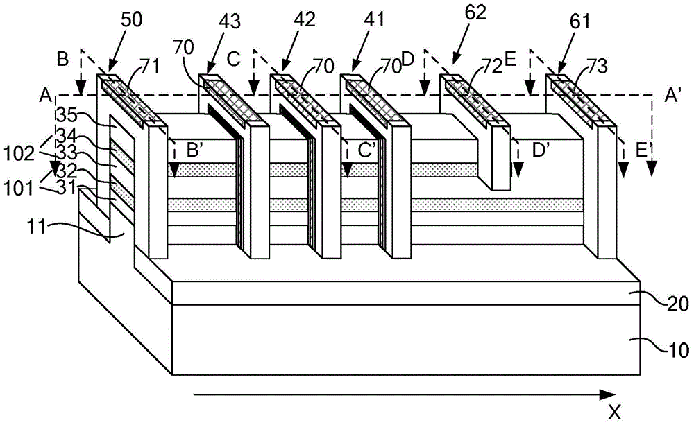
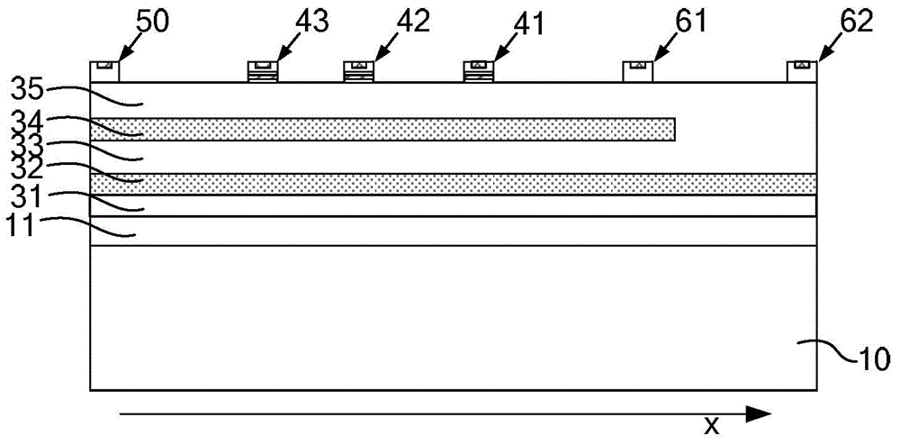
[0072] It can be seen from the background art that with the development of semiconductor devices, higher requirements are placed on the density of semiconductor devices on a wafer. In the prior art, the density of semiconductor devices is often increased by reducing the size of semiconductor devices. For example, in NAND memory, the density of NAND memory is increased by reducing the size of NAND memory. However, after the size of the NAND memory is reduced, problems such as read disturbance, transmission disturbance, programming disturbance, floating gate coupling, and hot carrier injection between NAND memories are more serious.

[0073] To this end, the present invention provides a semiconductor device and a method for forming the same. The semiconductor device includes:

[0074] fins protruding from the surface of the semiconductor substrate;

[0075] A multi-layer channel structure located on the fin and in a stacked structure, the channel structure including a channel ...


PUM


Abstract

The invention provides a semiconductor device and a forming method thereof. The semiconductor device comprises the processes as follows: a multi-layer channel structure in a stack structure is formed at the upper part of a fin of a semiconductor substrate; the channel structure comprises a channel insulating layer and channel layers located on the channel insulating layer; a plurality of drain structures stretching across the multi-layer channel structure are formed at the upper part of the multi-layer channel structure; the plurality of drain structures correspond to a plurality of channel layers one by one; and one drain structure covers the side wall of one channel layer. The structure of the semiconductor device is applied to NAND memories; one channel layer in the multi-layer channel structure is used for forming a memory unit; and the density of the NAND memories can be increased by the stacked channel layer structure under the condition of the same technical dimension, so that the continuous data density increase capacity of the semiconductor device is improved; and the problem of mutual performance interference between the adjacent NAND memories due to the fact that the size of the device is reduced to increase the density of the NAND memories in the prior art is solved.

Description

technical field [0001] The invention relates to the technology in the field of semiconductor manufacturing, in particular to a semiconductor device and a forming method thereof. Background technique [0002] Non-volatile memory is a type of semiconductor memory that continues to store data when power is removed. Among them, NAND memory is a kind of non-volatile memory commonly used, which has the advantages of small storage unit area and large storage capacity of the memory unit, so it is widely used in MP3 players, digital cameras, digital video recorders and mobile phones, etc. inside the memory card of a portable electronic product. [0003] figure 1 It is a schematic diagram of an existing NAND structure. figure 1 The middle NAND includes: a gate dielectric layer 3 arranged on a semiconductor substrate 1, a floating gate layer 4 positioned on the gate dielectric layer 3, and a control gate layer 6 positioned on the floating gate layer 4, in the control gate layer 6 A...

Claims


Application Information

Patent Timeline
Patent Type & Authority Applications(China)
IPC IPC(8): H01L27/115H01L21/8247
Inventor 黄新运肖磊沈磊刘崎徐烈伟刘红霞
Owner SHANGHAI FUDAN MICROELECTRONICS GROUP
Why Eureka
Try Eureka