QLED and fabrication method thereof

A light-emitting layer and electrode technology, which is applied in semiconductor/solid-state device manufacturing, electrical components, circuits, etc., can solve the problems of low carrier mobility and quantum dot light-emitting layer thickness, etc., to improve luminous efficiency and brightness, Reduced driving voltage and good application prospects

A light-emitting layer and electrode technology, which is applied in semiconductor/solid-state device manufacturing, electrical components, circuits, etc., can solve the problems of low carrier mobility and quantum dot light-emitting layer thickness, etc., to improve luminous efficiency and brightness, Reduced driving voltage and good application prospects

CN106328822AActive Publication Date: 2017-01-11TCL CORPORATION

Image

  • QLED and fabrication method thereof
  • QLED and fabrication method thereof
  • QLED and fabrication method thereof

Examples


Embodiment Construction

[0019] In order to make the technical problems, technical solutions and beneficial effects to be solved by the present invention clearer, the present invention will be further described in detail below with reference to the embodiments. It should be understood that the specific embodiments described herein are only used to explain the present invention, but not to limit the present invention.

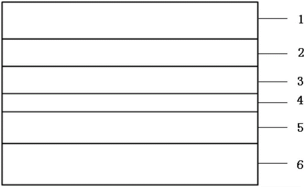
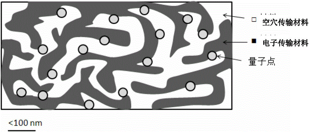
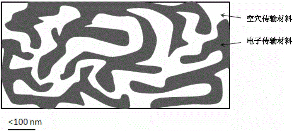
[0020] combine Figure 1-3 , an embodiment of the present invention provides a QLED, such as figure 1 As shown, it includes a first electrode 1, a hole injection layer 2, a hole transport layer 3, a light-emitting layer 4, an electron transport layer 5 and a second electrode 6 arranged in sequence, and the light-emitting layer 4 is composed of quantum dot light-emitting materials and mixed It is made of transport material, the mixed transport material is a hole transport material and an electron transport material, and the hole transport material and the electron transport material for...


PUM


Abstract

The invention provides a QLED, which comprises, in sequence, the first electrode, hole injection layer, hole transport layer, emitting layer, electron transport layer and the second electrode. The emitting layer comprises quantum dots luminescent materials and mixed transport materials. The mixed transport materials comprise hole transport material and electron transport material. The hole transport material and electron transport material form double continuous network structure in the emitting layer, with the quantum dots luminescent materials scattered in the double continuous network structure.

Description

technical field [0001] The invention belongs to the technical field of display, and in particular relates to a QLED and a preparation method thereof. Background technique [0002] Inorganic nanocrystalline quantum dot luminescent materials have the advantages of saturated color and adjustable wavelength of emitted light, and high photoluminescence and electroluminescence quantum yields, which are suitable for the preparation of high-performance display devices. In addition, from the perspective of preparation technology, quantum dot light-emitting materials can be prepared into films by solution processing methods such as spin coating, printing, and printing equipment under non-vacuum conditions. Therefore, quantum dot light-emitting diodes (QLEDs) prepared with quantum dot films have become strong competitors for next-generation display technologies. [0003] Generally, a QLED device includes an electrode 1 , a hole injection, transport layer, a light emitting layer, an el...

Claims


Application Information

Patent Timeline
11 Jan 2017
Publication
CN106328822A
IPC
H01L51/50; H01L51/54; H01L51/56
CPC
H10K85/111; H10K50/115; H10K2102/00; H10K71/00
Inventors
้™ˆๅดง; ้’ฑ็ฃŠ