Display device, backlight module and field emission light source device thereof

A light source device and field emission technology, applied in the direction of lamp components, etc., can solve the problems of serious heat generation, poor thermal conductivity, and shortened service life of field emission lighting devices.

Active Publication Date: 2017-01-18
NANJING CEC PANDA LCD TECH
View PDF3 Cites 3 Cited by
  • Summary
  • Abstract
  • Description
  • Claims
  • Application Information

AI Technical Summary

Problems solved by technology

[0005] In addition, field emission lighting devices generally use ITO (indium tin oxide) as the anode electrode layer, and phosphor as the luminescent material

Method used


Image

  • Display device, backlight module and field emission light source device thereof
  • Display device, backlight module and field emission light source device thereof

Examples


Embodiment approach

[0038] One of the specific implementation methods is as follows:

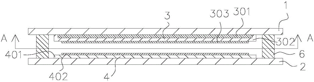
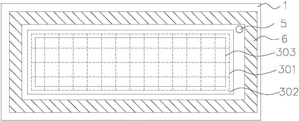
[0039]Make metal grid lines on the light emitting area on the white glass first. The physical vapor deposition process (PVD) is used to make the entire metal film. The metals are preferably Ti, Cu, W, Mo, Ag, Al, Au, Pt, Cu, etc., the target purity is >99.99%, and the film thickness is 10-100nm. Coat a layer of positive photoresist for TFT LCD on the metal film with a thickness of 1.5-5um. Using photolithography process, only the metal grid line pattern (pattern) in the light-emitting area is retained. The width of the metal line is 2-20um, accounting for less than the area of ​​the light-emitting area. More than 5%.

[0040] In addition to the method of using positive photoresist, it is also possible to coat a layer of negative photoresist on the white glass (positive photoresist can also be used, the precision is slightly worse than negative photoresist), and the film thickness is 1.5-5um. After a photolith...


PUM

PropertyMeasurementUnit
Line widthaaaaaaaaaa
Thicknessaaaaaaaaaa

Abstract

The invention discloses a display device, a backlight module and a field emission light source device thereof. The field emission light source device comprises an anode formed on a substrate, the anode including an anode electrode layer provided on the substrate, and a luminescent material layer disposed on the anode electrode layer wherein the anode electrode layer comprises: a thermally conductive layer on the substrate and a transparent conductive film on the thermally conductive layer. The luminescent material layer is arranged on the transparent conductive film. The thermally conductive layer is made of metal materials and has a grid structure. The invention also provides a backlight module and a display device with the field emission light source device. According to the invention, the problem with severe heating of a field emission light source device can be resolved.

Description

technical field [0001] The invention relates to the technical field of liquid crystal display, in particular to a field emission light source device, a backlight module and a display device with the field emission light source device. Background technique [0002] The advantages of liquid crystal displays such as clear picture quality, thin and light portability, low power consumption and long life make them become the mainstream of displays. Liquid crystal display requires a backlight source, currently mainly CCFL (Cold Cathode Fluorescent Lamp) and LED. CCFL is a line light source, and LED is a point light source, which requires light guide plates, reflectors, diffusers, etc. to disperse the light evenly. [0003] The field emission lighting device is a new type of planar light source, which has the advantages of high luminous efficiency, low power consumption, long life, thinness, and easy control. It is a promising backlight source for LCD displays. As a flat light sou...

Claims


Application Information

Patent Timeline
IPC IPC(8): H01J63/02
CPCH01J63/02
Inventor 徐竹青
Owner NANJING CEC PANDA LCD TECH
Why Eureka
Try Eureka