

Indium antimonide infrared focal plane array detector chip and manufacturing method thereof
An indium antimonide infrared focus and detector chip technology, applied in semiconductor devices, electrical components, circuits, etc., can solve problems such as low reliability, achieve optimal reliability and stability, reduce strain, and improve reliability. Effect
Active Publication Date: 2013-05-15
CHINA AIR TO AIR MISSILE INST
View PDF0 Cites 7 Cited by
- Summary
- Abstract
- Description
- Claims
- Application Information
AI Technical Summary
Problems solved by technology
In order to solve the problem of low reliability of the indium antimonide infrared focal plane array detector chip in the prior art, the present invention provides an indium antimonide infrared focal plane array detector chip with high reliability
Method used
View moreImage
Smart ImageViewing Examples

Examples
Embodiment Construction
Login to View More PUM
 Abstract
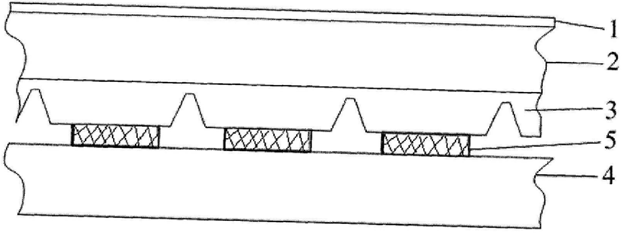
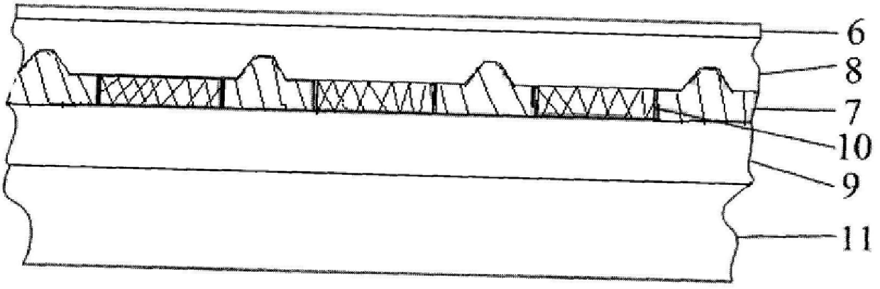
An indium antimonide infrared focal plane array detector chip, which includes an antireflection film [6], a low-temperature glue [7], an indium antimonide photosensitive array [8], a silicon readout circuit [9], and an indium column [10] , InSb substrate [11]. Wherein, the indium antimonide photosensitive array [8] is provided with an antireflection film [6] on the back, and an indium pillar [10] is provided on the front. The other end of the indium column [10] is connected to the silicon readout circuit [9], and the backside of the silicon readout circuit [9] is provided with an indium antimonide substrate [11], and the indium antimonide photosensitive array [8], the silicon A low-temperature glue [7] is arranged in the gap between the readout circuit [9] and the indium column [10]. The indium antimonide infrared focal plane array detector chip of the invention achieves thermal matching with the indium antimonide photosensitive array and the silicon readout circuit, reduces strain, and makes the indium antimonide infrared focal plane array detector have higher reliability. In addition, the invention provides a method for manufacturing the indium antimonide infrared focal plane array detector chip.
Description
Indium antimonide infrared focal plane array detector chip and manufacturing method thereof technical field The invention belongs to semiconductor photodetector manufacturing technology, and relates to an indium antimonide infrared focal plane array detector chip and a manufacturing method thereof. Background technique In the process of fabricating an InSb infrared focal plane array detector chip, structural design is a key process that determines the performance and reliability of the detector. The indium antimonide infrared focal plane array detector chip has to withstand the impact from normal temperature (300K) to liquid nitrogen temperature (77K) during testing and work. The thermal expansion coefficient of indium antimonide material is 5.04×10⁻⁶K, and the thermal expansion coefficient of silicon material The coefficient is 2.6×10⁻⁶K, and there is a large difference in the coefficient of thermal expansion between the two, so the stress caused by thermal mismatch is an...
Claims
Login to View More Application Information
Patent Timeline
 Patent Type & AuthorityPatents(China)
IPC IPC(8): H01L31/101H01L31/18
Inventor成彩晶吴伟付月秋曹光明张向锋李明华
OwnerCHINA AIR TO AIR MISSILE INST