

Preparation method of silicon dioxide dielectric film
A dielectric film, silicon dioxide technology, used in the manufacture of circuits, electrical components, semiconductor/solid-state devices, etc., can solve the problems of inability to meet the size of the microelectronic integrated circuit process, and achieve high gap filling performance and process stability. , Overcome the effect of insufficient filling
- Summary
- Abstract
- Description
- Claims
- Application Information
AI Technical Summary
Problems solved by technology
Method used
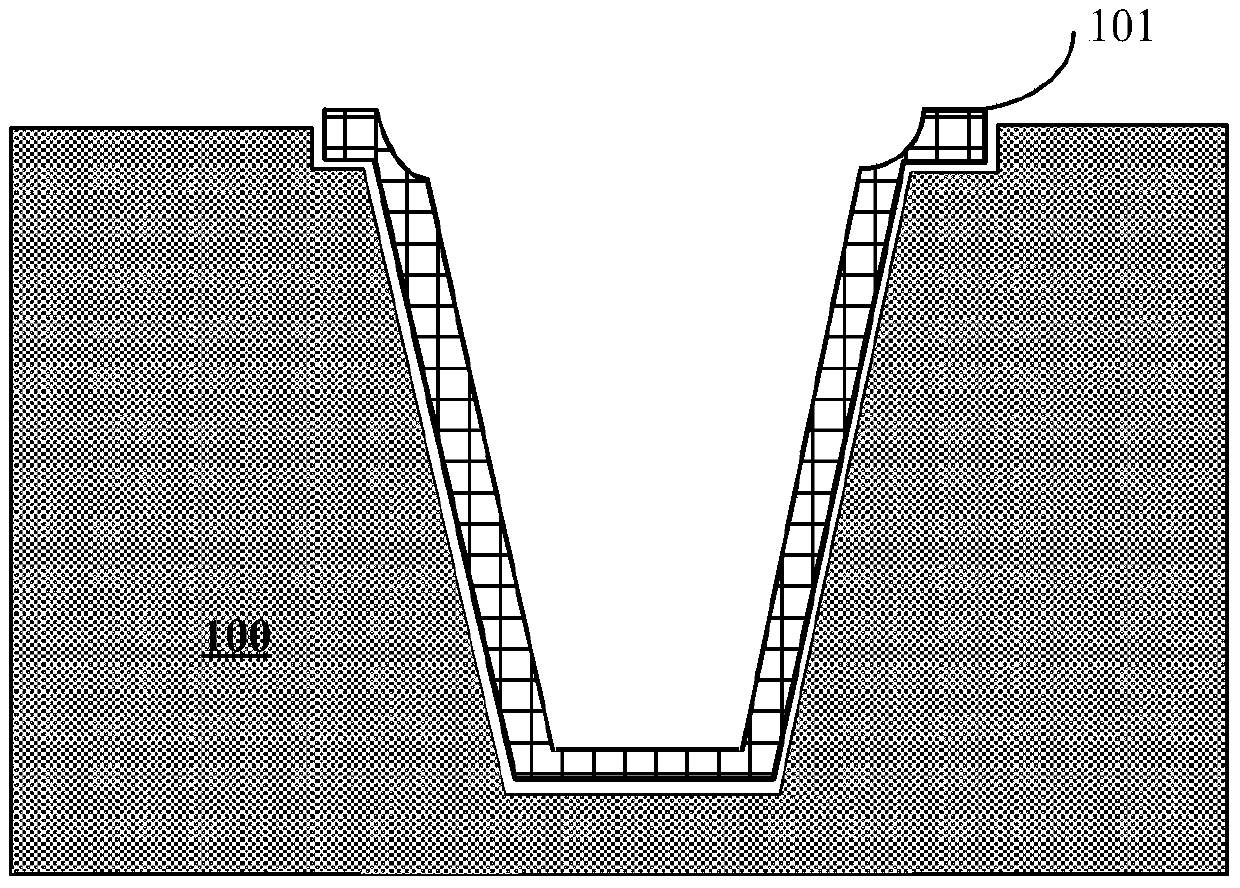
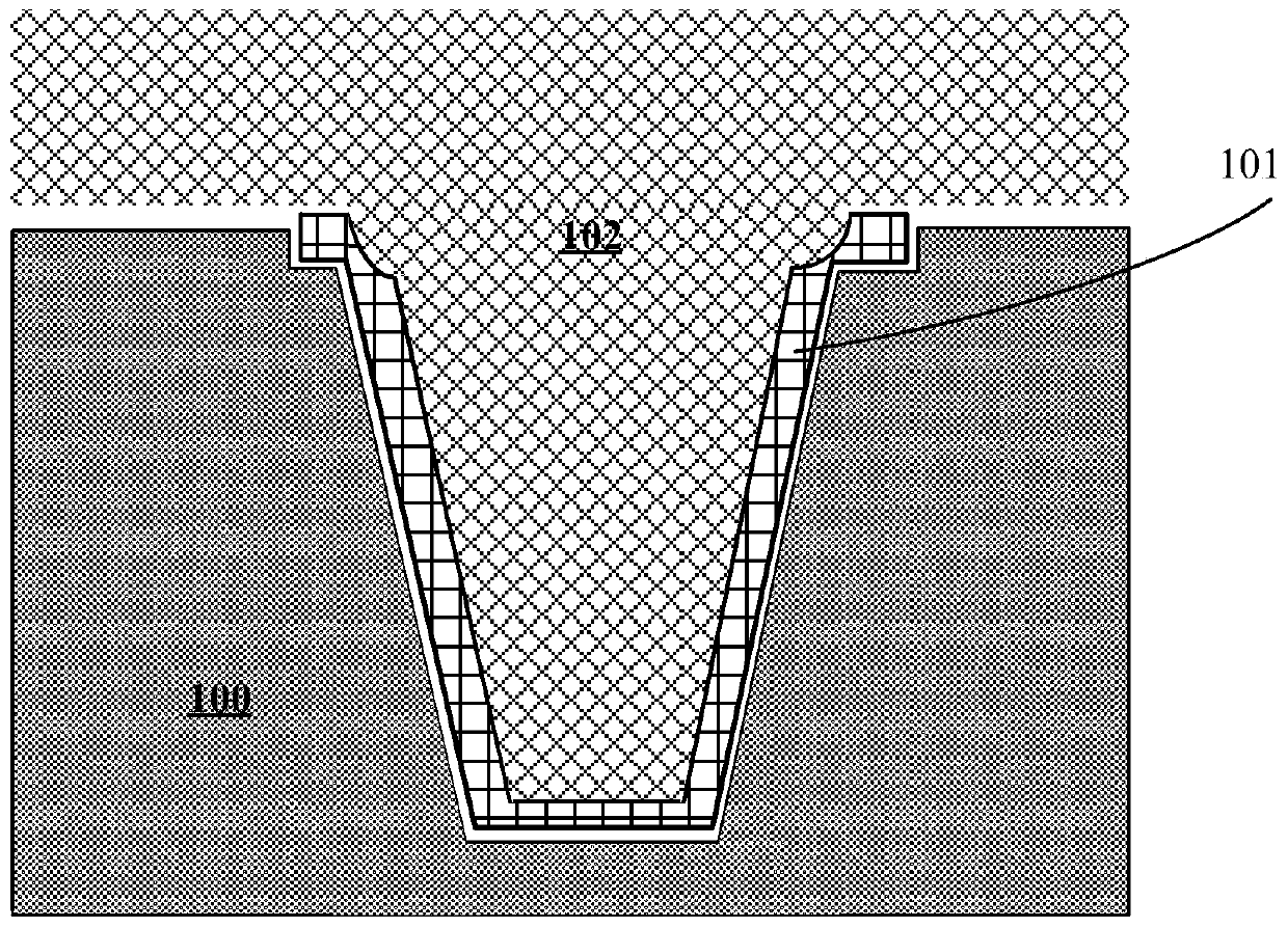
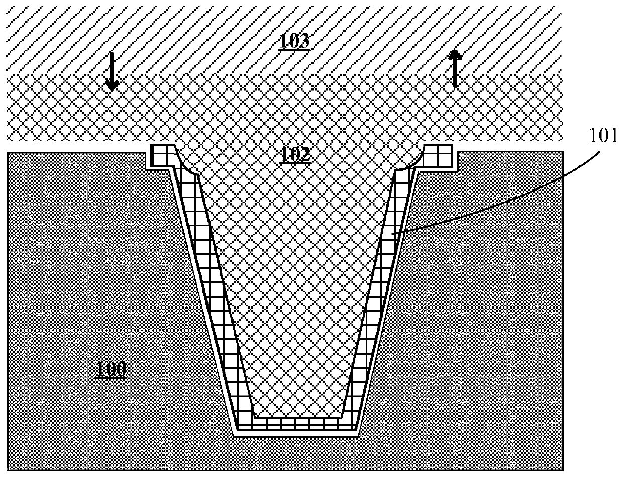
Image

Examples
Embodiment Construction
[0028] In the following description, numerous specific details are given in order to provide a more thorough understanding of the present invention. It will be apparent, however, to one skilled in the art that the present invention may be practiced without one or more of these details. In other examples, some technical features known in the art are not described in order to avoid confusion with the present invention.
[0029] It should be understood that the invention can be embodied in different forms and should not be construed as limited to the embodiments set forth herein. Rather, these embodiments are provided so that this disclosure will be thorough and complete, and will fully convey the scope of the invention to those skilled in the art.
[0030] In order to thoroughly understand the present invention, detailed steps and detailed structures will be provided in the following description, so as to explain the technical solution proposed by the present invention. Prefer...
PUM
| Property | Measurement | Unit |
|---|---|---|
| thickness | aaaaa | aaaaa |
Abstract
Description
Claims
Application Information