Transition loading plate device, display panel and manufacture method, minisize light-emitting member detection method

A manufacturing method and technology of light-emitting parts, which are applied in the direction of single semiconductor device testing, semiconductor/solid-state device manufacturing, semiconductor/solid-state device testing/measurement, etc., and can solve the problem of small size, excessively large probe size, and damage to micro-luminous light by probes Problems such as diodes to achieve the effect of improving yield

Active Publication Date: 2017-02-01
AU OPTRONICS CORP
View PDF5 Cites 34 Cited by
  • Summary
  • Abstract
  • Description
  • Claims
  • Application Information

AI Technical Summary

Problems solved by technology

However, compared with ordinary LEDs, micro-LEDs are smaller in size, so that the size of the probe is too large and it is not easy to contact the electrodes of the micro-LED

Method used


Image

  • Transition loading plate device, display panel and manufacture method, minisize light-emitting member detection method
  • Transition loading plate device, display panel and manufacture method, minisize light-emitting member detection method
  • Transition loading plate device, display panel and manufacture method, minisize light-emitting member detection method

Examples


Embodiment Construction

[0074] Below in conjunction with accompanying drawing, structural principle and working principle of the present invention are specifically described:

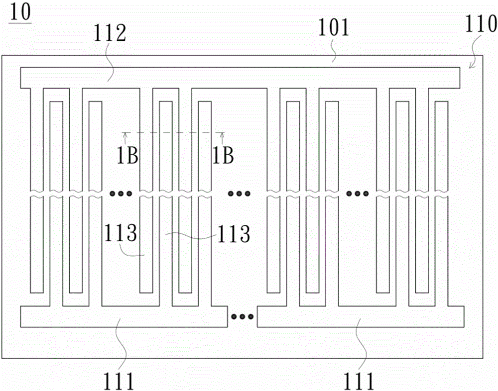
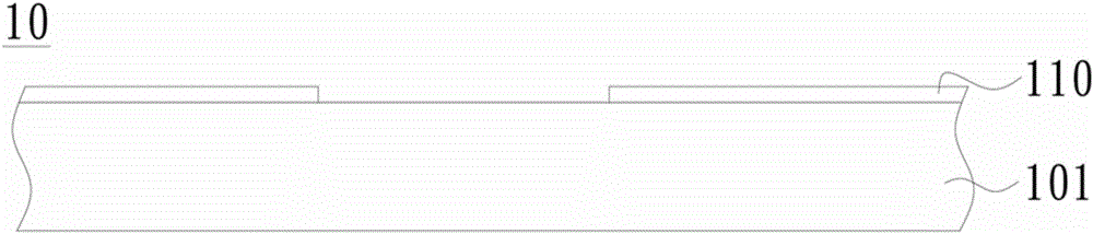
[0075] Figure 1A , Figure 1B , Figure 1C , Figure 1D , Figure 1E , Figure 1F , Figure 1G , Figure 1H , Figure 1I , Figure 1J , Figure 1K , Figure 1L , Figure 1M , Figure 1N and Figure 1O is a schematic diagram of a method for manufacturing a transition carrier device according to an embodiment of the present invention. see Figure 1A and Figure 1B , in the manufacturing method of the transition carrier device, firstly, the wiring layer 110 is formed on the substrate 101 to form the transition carrier 10 including the substrate 101 and the wiring layer 110 . Figure 1A shows a top view of the transition carrier 10, and Figure 1B for Figure 1A The cross-sectional view drawn along the line 1B-1B in the center.

[0076] The substrate 101 is preferably a rigid substrate, such as a glass plate or a c...


PUM


Abstract

The inventio discloses a transition loading plate device, s display panel and s manufacture method, and a minisize light-emitting member detection method. The transition plate device manufacture method comprises steps of forming a circuit layer, forming a support layer which has a plurality of openings exposing the circuit layers; the protection layer is formed on the support layer and covers the support layer and the circuit layer which is exposed by the opening; a pattern layer is adhered to the protection layer; at least one minisize light emitting member is adhered to the pattern layer; an insulation layer is formed on the protection layer ad the minisize light emitting member; after that, the protection layer and the insulation layer are removed in order to form a plurality of contact holes; then, a lead layer is formed on the insulation layer; and the light-emitting member and the circuit layer are electrically connected through the contact holes. Besides, the invention also discloses a transition loading plate device, a method for detecting the minisize light-emitting member, a display panel and a manufacture method for the same.

Description

technical field [0001] The present invention relates to a carrying device for an optic electronic component, a display device, a manufacturing method for both the carrying device and the display device, and a detection method for an optic electronic component, in particular to a method for carrying a micro light-emitting component (micro A transitional carrier device (temporary carrier device) for a light emitting device, a method for detecting micro-light-emitting devices using the transitional carrier device, a display panel (display panel) containing the micro-light-emitting device, and both the aforementioned transitional carrier device and the display panel manufacturing method. Background technique [0002] The current Solid-State Lighting technology (Solid-State Lighting, SSL) has developed a small-sized Micro Light Emitting Diode (μLED), the length or width of which can be below 10 micrometers (μm). For example, the bottom surface of a miniature LED may be a 10 micr...

Claims


Application Information

Patent Timeline
IPC IPC(8): H01L21/50H01L23/498H01L27/15H01L21/66
CPCH01L23/49838H01L27/15H01L21/50H01L22/14H01L33/0095H01L25/0753H01L33/62G01R31/2635
Inventor 何金原罗国隆吴宗典
Owner AU OPTRONICS CORP
Why Eureka
Try Eureka