Double-gate SCR structure design for ESD protection

A technology of structural design and metal gate, applied in electrical components, thyristors, electric solid devices, etc., can solve the problems of low sustaining voltage, high triggering voltage, ineffectively increasing the sustaining voltage, etc., and achieve the effect of reducing the triggering voltage

Inactive Publication Date: 2017-02-01
马利峰
View PDF0 Cites 2 Cited by
  • Summary
  • Abstract
  • Description
  • Claims
  • Application Information

AI Technical Summary

Problems solved by technology

Conventional SCR devices are difficult to be directly applied due to high trigger voltage and low sustain voltage
Although the low trigger voltage (LVT-SCR)

Method used


Image

  • Double-gate SCR structure design for ESD protection
  • Double-gate SCR structure design for ESD protection

Examples


Embodiment Construction

[0012] The specific implementation manners of the present invention will be described in detail below in conjunction with the accompanying drawings.

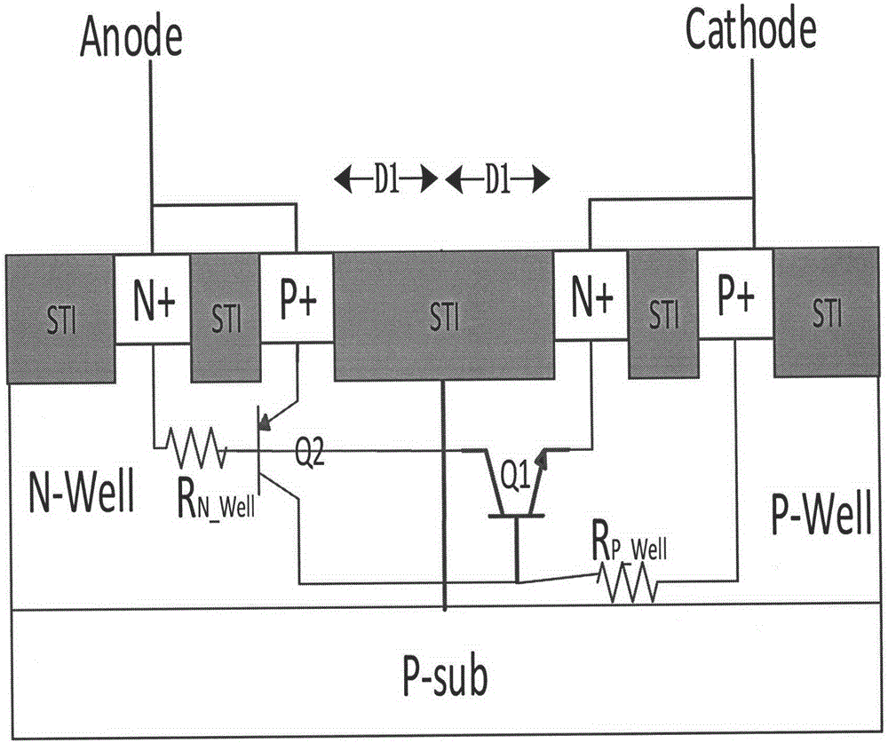
[0013] The sectional view and equivalent circuit diagram of the conventional SCR device in the prior art are as follows Figure 1 As shown, a conventional SCR is composed of two BJTs, in which P+ and N+ in N-Well are shorted and connected to Anode, and N+ and P+ in P-Well are shorted and connected to Cathode. Such a layout structure forms a PNP transistor Q2 and NPN transistor Q1 connected by positive feedback, when Cathode is grounded and a positive pulse appears on Anode, N-Well and P-Well form a reverse-biased PN junction, and when the reverse-biased voltage of the PN junction is high enough, it will occur Avalanche breakdown generates electron-hole pairs. The electrons and holes are collected by Anode and Cathode respectively, flow through the corresponding well resistance and generate a voltage drop, so that the Q1 and Q2 t...


PUM


Abstract

The invention, which belongs to the technical field of the integrated circuit, discloses a double-gate SCR structure design for ESD protection, wherein the structure has the excellent anti-latching performance. According to the designed double-gate SCR structure, a parasitic PMOS and a parasitic diode structure are introduced into a conventional SCR device, thereby reducing a device trigger voltage and increasing a maintaining voltage. The parasitic PMOS is formed by self-aligned injection of P+ heavily doping between two gates and combination of a substrate and two gates. Because of introduction of the device, the large hysteresis characteristic of the SCR can be reduced to a certain extent, thereby improving the maintaining voltage to a certain extent. Besides, the parasitic diode is from N+, P-Well, P+, and N-Well. On the basis of the structure, the trigger voltage of the device can be reduced effectively. When the IC chip is in a non-electrified state during production, packaging, and testing processes, the SCR structure is turned on and the high electrostatic protection capability is realized.

Description

technical field [0001] The present invention relates to the technical field of integrated circuits, more specifically, the present invention relates to SCR devices, in particular to an SCR structure used for electrostatic protection of IC chips. [0002] technical background [0003] In the process of IC chip production, packaging, testing, storage, and handling, it will be exposed to a large amount of external electrostatic charges, thereby forming the phenomenon of electrostatic discharge. Electrostatic discharge is ubiquitous as an unavoidable natural phenomenon. With the reduction of the feature size of integrated circuit technology and the development of various advanced technologies, it is more and more common for chips to be damaged by ESD phenomena. Relevant research and investigations have shown that 30% of integrated circuit failure products are caused by electrostatic discharge phenomena. caused. Therefore, it is very important to use high-performance ESD protect...

Claims


Application Information

Patent Timeline
IPC IPC(8): H01L27/02H01L29/74
CPCH01L27/0248H01L29/7404
Inventor 马利峰
Owner 马利峰
Why Eureka
Try Eureka