Field-programmable gate array chip-based process mapping method

A gate array and chip technology, applied in special data processing applications, instruments, electrical digital data processing, etc., can solve the problems of losing the ability to customize the FPGA chip architecture, spending a lot of time, and taking a long time to achieve the highest improvement The effect of working frequency, increasing fmax, and reducing cost

Inactive Publication Date: 2017-02-15
HERCULES MICROELECTRONICS CO LTD
View PDF5 Cites 3 Cited by
  • Summary
  • Abstract
  • Description
  • Claims
  • Application Information

AI Technical Summary

Problems solved by technology

[0003] However, in the process of process mapping of existing FPGA chips, there are always some problems. For example, some FPGA chips lose the ability to customize support for each FPGA chip architecture because they are too general for various algorithms. ; Some FPGA chips are optimized for the details of the FPGA chip architecture, and when the FPGA chip architecture changes, in order to support the new architecture, it takes a lot of time to rewrite the algorithm under the architecture
[0004] It can be seen that the existing process mapping process cannot perform timely and corresponding processing for different FPGA chip architectures, resulting in long time-consuming or inability to complete the mapping process and other problems.

Method used


Image

  • Field-programmable gate array chip-based process mapping method
  • Field-programmable gate array chip-based process mapping method
  • Field-programmable gate array chip-based process mapping method

Examples


Embodiment Construction

[0015] The technical solutions of the present invention will be described in further detail below with reference to the accompanying drawings and embodiments.

[0016] The process mapping method based on the field programmable gate array FPGA chip provided by the present invention is applied in the mapping process after the logic synthesis process in the process flow of the FPGA chip. The method can retain the versatility of the process mapping algorithm to the greatest extent, and can quickly Supports the different characteristics of various new FPGA chip architectures. The following will introduce in detail through the embodiments.

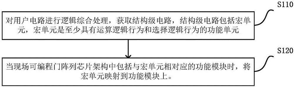
[0017] figure 1 A flow chart of a process mapping method based on a field programmable gate array chip provided by an embodiment of the present invention, such as figure 1 As shown, the method may include:

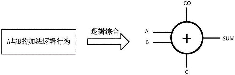
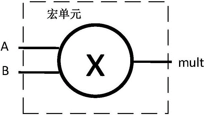
[0018] Step 110, perform logical synthesis processing on the user circuit to obtain a structural level circuit, the structural level cir...


PUM


Abstract

The embodiment of the invention provides a field-programmable gate array chip-based process mapping method. According to the method, a structure level circuit can be obtained through logic synthesis processing on a user circuit; the structure level circuit comprises a macroelement; and the macroelement is a function unit which at least comprises an operating logic behavior and a selecting logic behavior. When a field-programmable gate array chip architecture comprises a function module corresponding to the macroelement, the macroelement is mapped to the function module. According to the method, the universality of a process mapping algorithm can be reserved to the maximal extent; and different characteristics of multiple novel FPGA chip architectures can also be quickly supported, so that the time cost and the space (a software memory) cost are reduced; and the maximum work frequency fmax of an overall FPGA chip is improved.

Description

technical field [0001] The present invention relates to the technical field of integrated circuits, in particular to a process mapping method based on a field programmable gate array chip Background technique [0002] Field Programmable Gate Array (Field Programmable Gate Array, FPGA) chip is a logic device with abundant hardware resources, powerful parallel processing capability and flexible reconfigurable capability. These features make FPGA more and more widely used in data processing, communication, network and many other fields. [0003] However, in the process of process mapping of existing FPGA chips, there are always some problems. For example, some FPGA chips lose the ability to customize support for each FPGA chip architecture because they are too general for various algorithms. ; Some FPGA chips are too optimized for the details of the FPGA chip architecture, and when the FPGA chip architecture changes, in order to support the new architecture, it takes a lot of ...

Claims


Application Information

Patent Timeline
Patent Type & Authority Applications(China)
IPC IPC(8): G06F17/50
CPCG06F30/34
Inventor 耿嘉樊平
Owner HERCULES MICROELECTRONICS CO LTD
Why Eureka
Try Eureka