Manufacturing method and test circuit of a semiconductor device

A manufacturing method and a technology for testing circuits, which are applied in semiconductor/solid-state device testing/measurement, semiconductor devices, semiconductor/solid-state device components, etc., and can solve problems such as the influence of transistor electrical parameters

Active Publication Date: 2019-04-16
WUXI CHINA RESOURCES HUAJING MICROELECTRONICS
View PDF6 Cites 0 Cited by
  • Summary
  • Abstract
  • Description
  • Claims
  • Application Information

AI Technical Summary

Problems solved by technology

[0007] The invention provides a manufacturing method and a test circuit of a semiconductor device to solve the problem that the electrical parameters of the transistor are affected by ESD in the prior art

Method used


Image

  • Manufacturing method and test circuit of a semiconductor device
  • Manufacturing method and test circuit of a semiconductor device
  • Manufacturing method and test circuit of a semiconductor device

Examples


Embodiment Construction

[0033] In order to make the purpose, technical solutions and advantages of the present invention clearer, the technical solutions of the present invention will be clearly and completely described through implementation with reference to the accompanying drawings in the embodiments of the present invention. Obviously, the described embodiments are the embodiment of the present invention. Some, but not all, embodiments. Based on the embodiments of the present invention, all other embodiments obtained by persons of ordinary skill in the art without making creative efforts belong to the protection scope of the present invention.

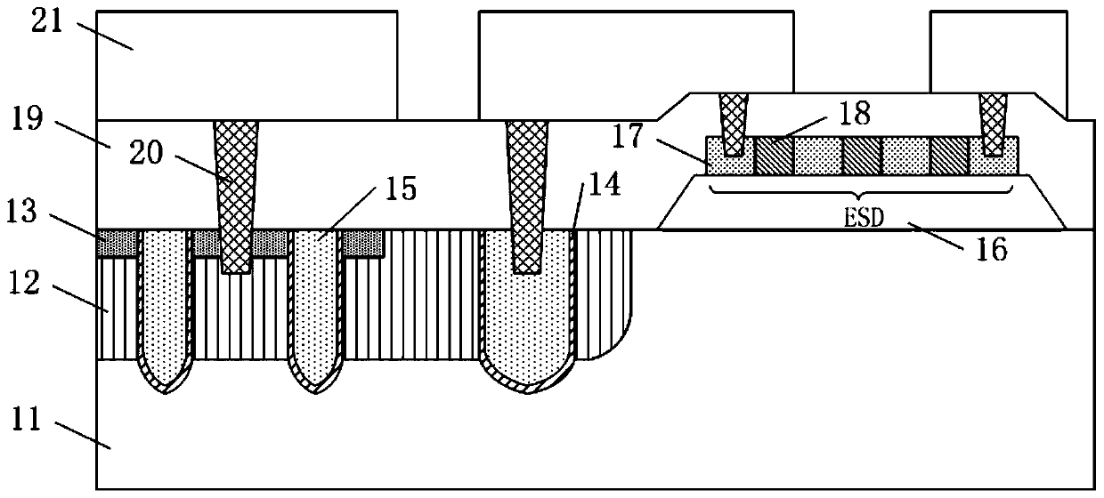
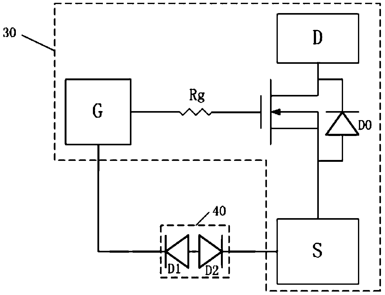
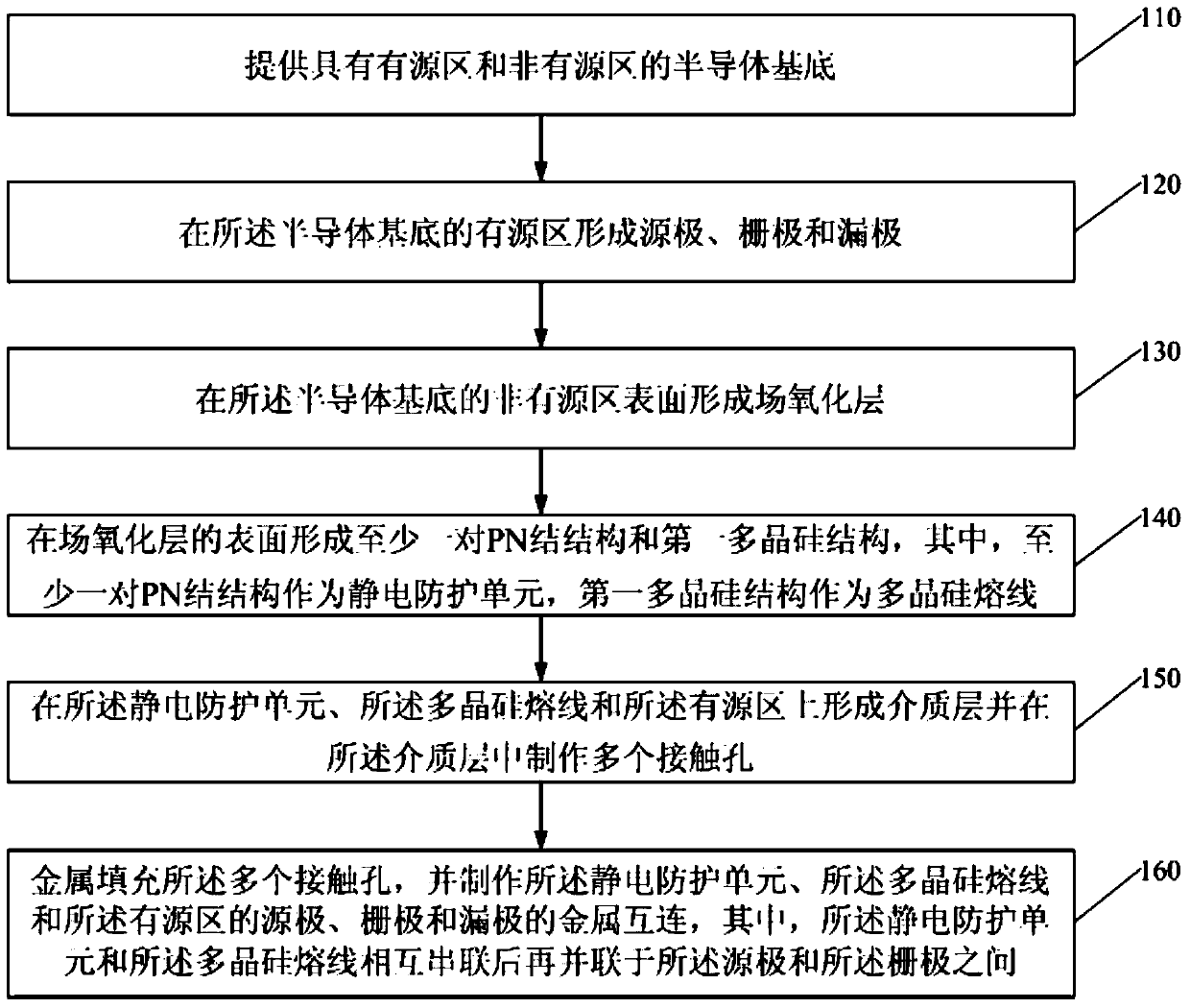
[0034] refer to Figure 2a As shown, it is a flow chart of a semiconductor device manufacturing method provided by Embodiment 1 of the present invention, for a clearer description Figure 2a , refer to here Figure 2b , is a structural diagram of a semiconductor device provided in Embodiment 1 of the present invention. The technical solution of this e...


PUM


Abstract

The present invention discloses a semiconductor device manufacturing method and a semiconductor device test circuit. The method comprises the steps of providing a semiconductor substrate having an active area and a non-active area; forming a source, a grid and a drain in the active area of the semiconductor substrate; forming a field oxide layer on the surface of the non-active area of the semiconductor substrate; forming at least one pair of PN-junction structure and a first polysilicon structure on the surface of the field oxide layer, wherein the at least one pair of PN-junction structure is used as an electrostatic protection unit, and the first polysilicon structure is used as a polysilicon fuse wire; forming the dielectric layers on the electrostatic protection unit, the polysilicon fuse wire and the active area, and making a plurality of contact holes in the dielectric layers; filling the plurality of contact holes with metals, and making the metal interconnection of the electrostatic protection unit, the polysilicon fuse wire and the source, the grid and the drain of the active area, wherein the electrostatic protection unit and the polysilicon fuse wire are connected in series and then are in parallel connection between the source and the grid. According to the present invention, the real electrical parameters of the transistors in a semiconductor device and the electrical parameter of the electrostatic protection unit are detected effectively.

Description

technical field [0001] The invention relates to a semiconductor manufacturing process, in particular to a manufacturing method and a testing circuit of a semiconductor device. Background technique [0002] Static electricity and electrostatic discharge are ubiquitous in daily life, but for electronic devices, a slight discharge that cannot be detected by the human body may cause serious damage or failure of the electronic device, or, when the electronic device is placed alone or packed into a circuit module, Even without power, static electricity can cause permanent damage to devices. Therefore, in existing electronic devices, components sensitive to electrostatic discharge, such as integrated circuits and transistors, all have an electrostatic protection (Electron Static Discharge, ESD) design. [0003] Taking N-type MOSFET (Metal-Oxide-Semiconductor Field Effect Transistor) as an example, refer to Figure 1a As shown, it is a sectional view of an NMOSFET with ESD provided...

Claims


Application Information

Patent Timeline
Patent Type & Authority Patents(China)
IPC IPC(8): H01L23/60H01L23/525H01L21/66
Inventor 张雨岳玲
Owner WUXI CHINA RESOURCES HUAJING MICROELECTRONICS
Why Eureka
Try Eureka