Touch display panel, manufacturing method thereof, and touch display device

A technology for a touch display panel and a manufacturing method, which are applied in the fields of instruments, computing, electrical digital data processing, etc., can solve the problems of the polarizer being easily affected by a humid environment, the problem that the polarizer is not easily affected by moisture, and the process and manufacturing costs are increased. , to avoid being susceptible to moisture, improve the aspect ratio, and achieve the effect of low cost

Active Publication Date: 2019-03-08
GUANGZHOU GOVISIONOX TECH CO LTD
View PDF10 Cites 0 Cited by
  • Summary
  • Abstract
  • Description
  • Claims
  • Application Information

AI Technical Summary

Problems solved by technology

When the display screen is an OLED (Organic Light-Emitting Diode, Organic Light-Emitting Diode) display screen, in order to reduce the influence of external light on the OLED display screen, a circular polarizer is generally arranged between the touch screen and the OLED display screen. Although this structure It can effectively eliminate the influence of the outside world on the OLED display, but it increases the overall thickness, which is not conducive to the thinning of the device, and the centerline part of the polarizer (PVA layer) is easily affected by the humid environment, which affects the display effect of the display.
And the touch screen will increase the thickness of the display device, increase the process and manufacturing cost
[0004] In the prior art, in order to meet the thinning requirements of products, the touch control circuit is generally placed inside the display panel (oncell), or the touch control circuit is placed on the display panel (incell), or the touch control circuit is integrated into the polarizer In the glue layer, although the thickness of the display can be reduced to a certain extent, it cannot solve the unfavorable factors such as the polarizer is not easy to be affected by moisture.

Method used


Image

  • Touch display panel, manufacturing method thereof, and touch display device
  • Touch display panel, manufacturing method thereof, and touch display device
  • Touch display panel, manufacturing method thereof, and touch display device

Examples


Embodiment 1

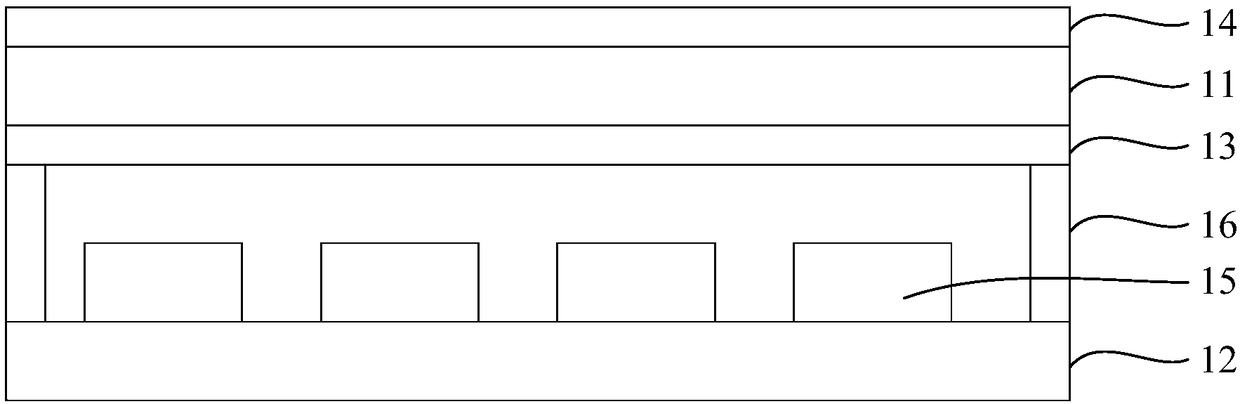
[0038] Please refer to figure 1 and figure 2 , which is a schematic structural diagram of the touch display panel provided in Embodiment 1 of the present invention. Such as figure 1 and figure 2 As shown, the touch display panel includes: a first substrate 11 and a second substrate 12 oppositely arranged, a nano-metal grating 14 located on the first substrate 11 away from the second substrate 12, located on the The organic light-emitting layer 15 on the second substrate 12 close to the first substrate 11 side, and the retardation film 13 between the nano-metal grating 14 and the organic light-emitting layer 15; the retardation film 13 and the organic light-emitting layer 15 The nano-metal grating 14 constitutes a circular polarizer, and the nano-metal grating 14 is divided into at least one mutually conductive grating unit, and the at least one mutually conductive grating unit constitutes a touch sensor.

[0039] In this embodiment, the nano-metal grating 14 is located o...

Embodiment 2

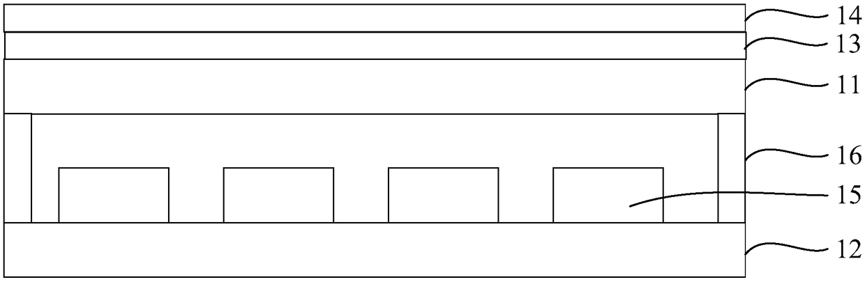
[0048] On the basis of Embodiment 1, the metal nano grating is located on the side of the first substrate close to the second substrate, and the phase difference film is located between the metal nano grating and the organic light-emitting layer .

[0049] Please refer to Figure 4 , which is a schematic structural diagram of the touch display panel provided in Embodiment 2 of the present invention. Such as Figure 4 As shown, the touch display panel includes: a first substrate 21 and a second substrate 22 oppositely arranged, a nano-metal grating 24 located on the first substrate 21 close to the side of the second substrate 22, located on the The organic light-emitting layer 25 on the second substrate 22 close to the first substrate 21 side, the retardation film 23 between the nano-metal grating 24 and the organic light-emitting layer 25; the retardation film 23 and the organic light-emitting layer 23 The nano-metal grating 24 constitutes a circular polarizer, and the nano...

Embodiment 3

[0058] Please refer to Figure 6 , which is a flow chart of the manufacturing method of the touch display panel provided by the third embodiment of the present invention. Such as Figure 6 As shown, the manufacturing method of the touch display panel includes the following steps:

[0059] Step S01: providing a first substrate, forming a nano-metal grating on the first substrate, and the nano-metal grating is composed of at least one mutually conductive grating unit;

[0060] Step S02: providing a second substrate, and forming an organic light-emitting layer on the second substrate;

[0061] Step S03: attaching the side of the second substrate on which the organic light-emitting layer is formed and the side of the first substrate away from the metal nano grating.

[0062] The touch display panel formed according to the manufacturing method of the touch display panel provided in this embodiment is as described in the first embodiment. Please refer to Figure 6 shown, combin...


PUM


Abstract

The invention provides a touch display panel, a manufacturing method thereof and a touch display device. The touch display panel comprises a first substrate, a second substrate, a nano metal grating, an organic light emitting layer and a phase difference piece, wherein the first substrate and the second substrate are arranged oppositely, the nano metal grating is located at the position, away from or close to one side of the second substrate, of the first substrate, the organic light emitting layer is located at the position, close to one side of the first substrate, of the second substrate, and the phase difference piece is located between the nano metal grating and the phase difference piece; a round polaroid is formed by the phase difference piece and the nano metal grating, and the nano metal grating is divided into at least one grating unit communicated mutually to form a touch sensor. The purpose of integrating the round polaroid and the touch sensor is achieved, the thickness of the displayer is reduced, manufacturing cost is reduced, and adverse factors caused by polaroid can be avoided, for example, the polaroid is prone to being affected with damp.

Description

technical field [0001] The present invention relates to the field of flat panel display, in particular to a touch display panel, a manufacturing method thereof, and a touch display device. Background technique [0002] The touch display can be operated only by the user touching the graphics or text on the display with his finger, which makes the human-computer interaction more straightforward. Today, touch displays have been widely used in the field of display technology. [0003] OSG (One Glass Solution, integrated touch) technology is an important touch technology. An OSG touch display generally includes a touch screen and a display screen. When the display screen is an OLED (Organic Light-Emitting Diode, Organic Light-Emitting Diode) display screen, in order to reduce the influence of external light on the OLED display screen, a circular polarizer is generally arranged between the touch screen and the OLED display screen. Although this structure It can effectively elim...

Claims


Application Information

Patent Timeline
Patent Type & Authority Patents(China)
IPC IPC(8): G06F3/041
CPCG06F3/041G06F3/0412G06F2203/04103
Inventor 刘仁杰
Owner GUANGZHOU GOVISIONOX TECH CO LTD
Why Eureka
Try Eureka