Manufacturing method of copper interconnection structure, copper interconnection structure and electronic device

A technology of copper interconnection structure and manufacturing method, which is applied in the direction of circuits, electrical components, electrical solid devices, etc., can solve the problems of device electrical performance degradation, interconnection resistance increase, RC delay increase, etc., to improve electrical performance, Effect of Reducing Interconnect Resistance

Active Publication Date: 2019-12-31
SEMICON MFG INT (SHANGHAI) CORP +1
View PDF6 Cites 0 Cited by
  • Summary
  • Abstract
  • Description
  • Claims
  • Application Information

AI Technical Summary

Problems solved by technology

[0003] In the copper interconnection process of the back-end process (BEOL), as the size of the device shrinks, the volume of copper used for interconnection is also reduced, and the reduction in copper volume and the size effect will cause the interconnection resistance to increase, and the device Electrical degradation issues (i.e., increased RC delay)
In order to reduce the increase in interconnect resistance due to the reduction in copper volume and size effects, various methods have been tried, one of the most promising methods is to reduce the metal liner between the copper and the dielectric layer. thickness, but this approach requires the introduction of materials with high step coverage, high diffusion resistance to copper and ULK (ultra-low K) oxides, which are not readily available and / or or preparation

Method used


Image

  • Manufacturing method of copper interconnection structure, copper interconnection structure and electronic device
  • Manufacturing method of copper interconnection structure, copper interconnection structure and electronic device
  • Manufacturing method of copper interconnection structure, copper interconnection structure and electronic device

Examples


Embodiment 1

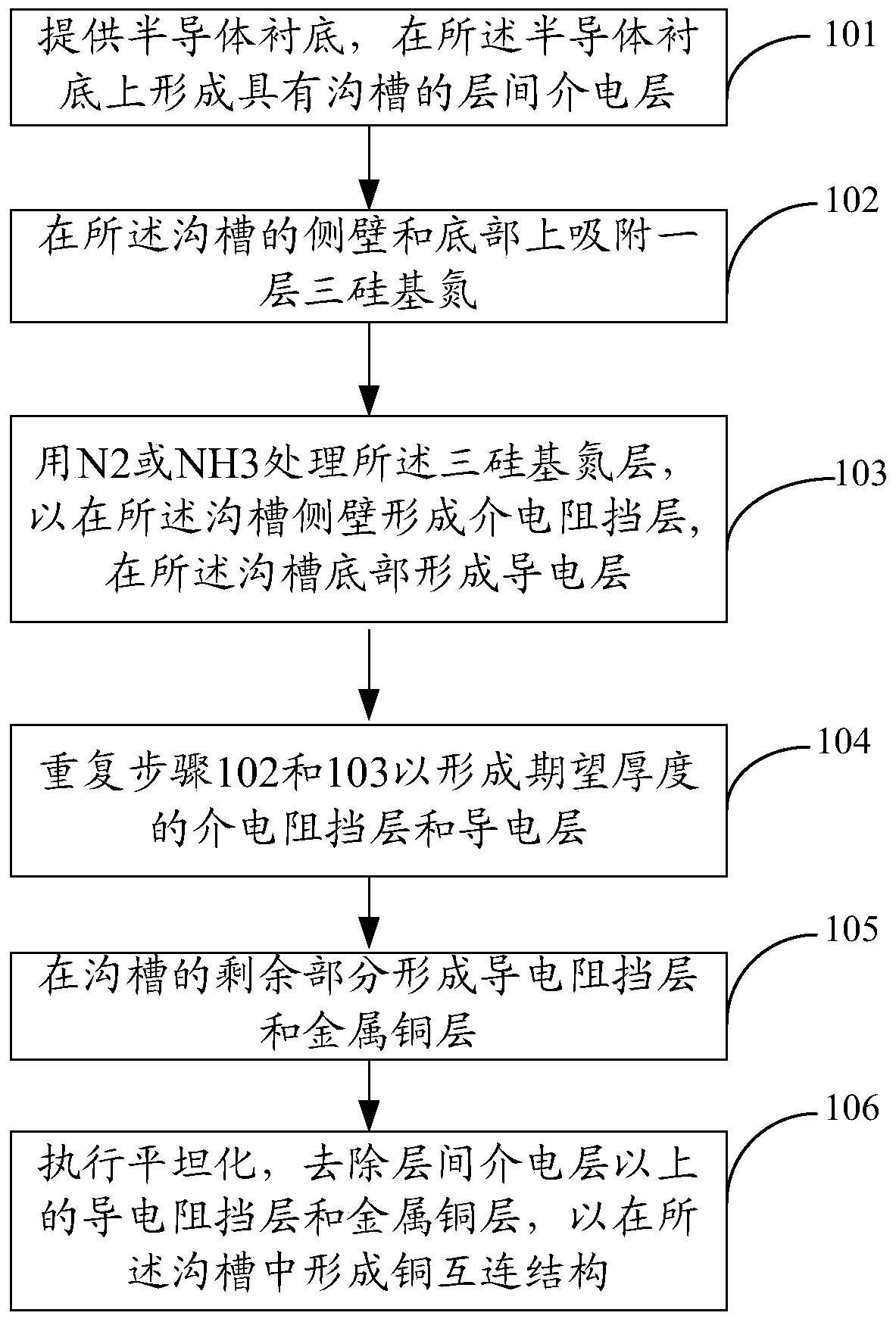
[0033] The following will refer to figure 1 as well as Figure 2A ~ Figure 2F A method for fabricating a copper interconnection structure according to an embodiment of the present invention is described in detail.

[0034] First, step S101 is performed to provide a semiconductor substrate on which an interlayer dielectric layer having a trench is formed.

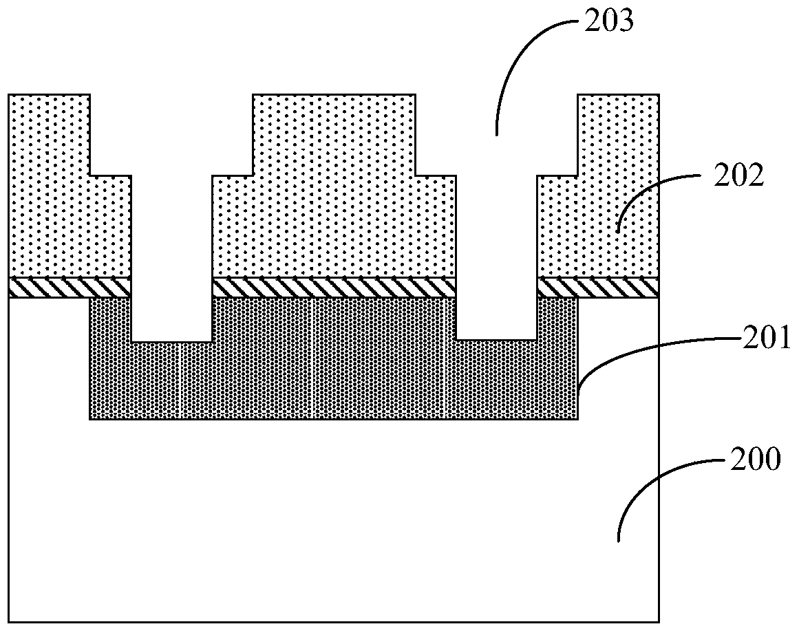
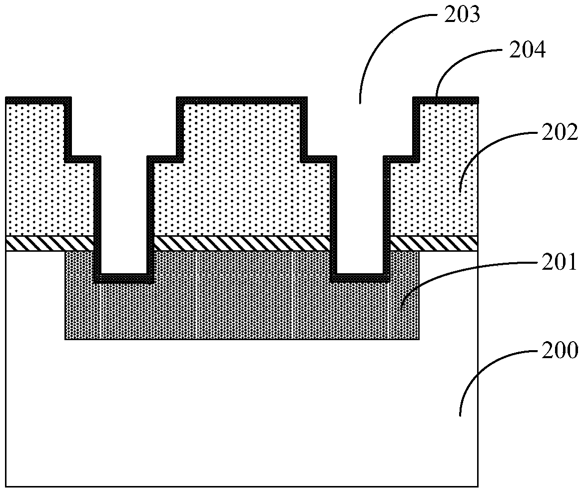
[0035] Such as Figure 2A As shown, a semiconductor substrate 200 is provided on which an interlayer dielectric layer 202 having a trench 203 is formed.

[0036]The semiconductor substrate 200 can be at least one of the materials mentioned below: Si, Ge, SiGe, SiC, SiGeC, InAs, GaAs, InP or other III / V compound semiconductors, and also includes multilayer structures composed of these semiconductors etc. or silicon-on-insulator (SOI), silicon-on-insulator (SSOI), silicon-germanium-on-insulator (S-SiGeOI), silicon-germanium-on-insulator (SiGeOI), and germanium-on-insulator (GeOI). Devices, such as NMOS and / or PMOS, can be ...

Embodiment 2

[0050] The present invention also provides a semiconductor device manufactured by the method described in Embodiment 1 or 2, which includes: a semiconductor substrate 300, an interlayer dielectric layer 301 with a groove formed on the semiconductor substrate 300 , a dielectric barrier layer 302, a conductive barrier layer 303, and a copper layer 304 filling the remaining part of the trench are sequentially formed on the sidewall of the trench.

[0051] Wherein, the semiconductor substrate 300 can be at least one of the materials mentioned below: Si, Ge, SiGe, SiC, SiGeC, InAs, GaAs, InP or other III / V compound semiconductors, and also includes multiple semiconductors composed of these semiconductors. The layer structure or the like may be silicon-on-insulator (SOI), silicon-on-insulator (SSOI), silicon-germanium-on-insulator (S-SiGeOI), silicon-germanium-on-insulator (SiGeOI), and germanium-on-insulator (GeOI). Devices, such as NMOS and / or PMOS, can be formed on the semiconduc...

Embodiment 3

[0055] The present invention further provides an electronic device including the aforementioned semiconductor device.

[0056] The electronic device also has the above-mentioned advantages due to the higher performance of the included semiconductor devices.

[0057] The electronic device can be any electronic product or equipment such as mobile phone, tablet computer, notebook computer, netbook, game console, TV, VCD, DVD, navigator, camera, video camera, recording pen, MP3, MP4, PSP, etc. It is an intermediate product with the above-mentioned semiconductor device, for example: a mobile phone motherboard with the integrated circuit, etc.


PUM


Abstract

The invention provides a copper interconnection structure manufacturing method, copper interconnection structure and electronic device wherein the manufacturing method comprises: providing a semiconductor substrate; forming on the semiconductor substrate an interlayer dielectric layer with groove; forming on the side wall of the groove a dielectric barrier layer; forming on the dielectric barrier layer a conductive barrier layer; and filling copper into the remaining part of the groove to form the copper interconnection structure. According to the copper interconnection structure manufacturing method provided by the invention, through the use of two barrier layers of the dielectric barrier layer and the conductive barrier layer, it is possible to ensure certain resistance capability and prevent copper from spreading to the dielectric barrier layer; and at the same time, it is possible to properly reduce the thickness of the conductive barrier layer so that the thickness of the copper layer for interconnection is increased in relative, therefore, further reducing the interconnection resistance and increasing the optical performance of a component.

Description

technical field [0001] The present invention relates to the technical field of semiconductors, in particular to a semiconductor device, a manufacturing method thereof, and an electronic device. Background technique [0002] With the development of semiconductor technology, integrated circuits are gradually developing towards ultra-large-scale integrated circuits (ULSI), and the feature size of the internal circuits is getting smaller and smaller, the density is getting higher and higher, and the number of components contained is increasing. With its excellent conductivity, copper has become one of the solutions for interconnection integration technology in the field of integrated circuit technology. [0003] In the copper interconnection process of the back-end process (BEOL), as the size of the device shrinks, the volume of copper used for interconnection is also reduced, and the reduction in copper volume and the size effect will cause the interconnection resistance to inc...

Claims


Application Information

Patent Timeline
Patent Type & Authority Patents(China)
IPC IPC(8): H01L21/768H01L23/528
CPCH01L21/768H01L21/76831H01L21/76832H01L23/528H01L23/53233H01L23/53295
Inventor 邓浩
Owner SEMICON MFG INT (SHANGHAI) CORP
Why Eureka
Try Eureka