Multilayer PCB positive back etching process

A process and etching technology, which is applied in the field of PCB manufacturing, can solve the problems of unfavorable electrical connection reliability, unobvious etch performance, slow erosion rate, etc., and achieve the desired effect of etch etch

Inactive Publication Date: 2017-03-22
JIANGMEN SUNTAK CIRCUIT TECH
View PDF5 Cites 7 Cited by
  • Summary
  • Abstract
  • Description
  • Claims
  • Application Information

AI Technical Summary

Problems solved by technology

[0005] Potassium permanganate method has a higher resin bite rate on the hole wall of multilayer PCB than glass fiber, the overall bite rate is slower, and the etchback performance is not obvious, so it is not suitable for the etchback process of multilayer PCB
[0006] The resin bite rate of the plasma deglue method on the hole wall of the multi-layer PCB is significantly higher than that of the glass fiber, which will cause pits on the hole wall, and then form a stepped hole wall during the metallization process of the hole wall, which is not conducive to the electrical connection between the inner and outer layers. Reliability, can not meet the requirements of multi-layer PCB etch back process

Method used


Image

  • Multilayer PCB positive back etching process

Examples


Embodiment 1

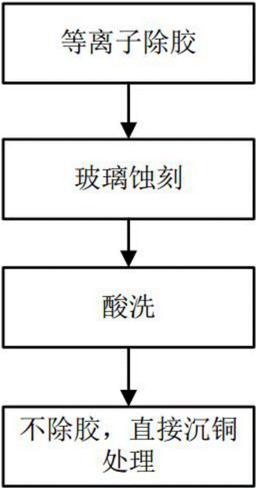
[0034] In the process of plasma degumming in step S1, the mixed gas of nitrogen, oxygen and hydrogen tetrafluoride is ionized with the electrode power of 7500-8500W, so that it reacts with the hole wall of the PCB through hole; The etchback reaction occurs on the wall of the through hole.

[0035] In this embodiment, preferably, the electrode power is 8000W.

Embodiment 2

[0037] During the plasma degumming process in step S1, the gas flow rate of nitrogen is 145-175 sccm, the gas flow rate of oxygen is 1100-1300 sccm, the gas flow rate of carbon tetrafluoride is 215-265 sccm, and the reaction time is 14-16 min.

[0038] In this embodiment, preferably, after mixing 160 sccm of oxygen, 1200 sccm of oxygen, and 240 sccm of carbon tetrafluoride, the mixed gas is ionized, and the PCB is ionized and etched for 15 minutes.

Embodiment 3

[0040] During the plasma degumming process in step S1, the flow rate of argon gas is 2700-3300 sccm, and the reaction time is 27-33 minutes.

[0041] In this embodiment, preferably, 3000 sccm argon gas is ionized, and the PCB is ionized and etched for 30 minutes.


PUM


Abstract

The invention relates to the PCB manufacturing field and provides a multilayer PCB positive back etching process. According to the multilayer PCB positive back etching process, plasma adhesive cleaning processing on a PCB after a boring flow is carried out, secondly, glass etching processing is then carried out, and lastly, PCB manufacturing is accomplished according to the technology in the prior art. The process is advantaged in that through combining two etching modes of plasma adhesive cleaning and glass etching, glass fiber and epoxy resin in a prepreg of the PCB are enabled to reach a relatively balance fretting rate in an etching process, and a relatively ideal back etching effect is realized.

Description

technical field [0001] The invention relates to the field of PCB manufacturing, in particular to a process for positive recessing of multilayer PCBs. Background technique [0002] PCB (short for Printed Circuit Board) is also known as printed circuit board. With the rapid development of electronic technology, especially aerospace and military products, due to their extremely harsh application environment, the requirements for the accuracy and reliability of PCBs are also more stringent. Generally, such products require the use of PCBs produced by the etch process. [0003] In the PCB manufacturing process, in order to facilitate the electrical connection between the inner and outer layers of the multi-layer PCB, the multi-layer PCB must be drilled, and then the hole wall is metallized through sinking copper and full-board electroplating, so as to realize the various layers of the PCB. electrical connection between. However, during the drilling process of multi-layer PCB, d...

Claims


Application Information

Patent Timeline
Patent Type & Authority Applications(China)
IPC IPC(8): H05K3/00
CPCH05K3/0085H05K2203/0789H05K2203/095
Inventor 黄力王海燕张义兵汪广明
Owner JIANGMEN SUNTAK CIRCUIT TECH
Why Eureka
Try Eureka