Solar cell photoluminescence high-speed detection system based on short-wave infrared imager and operation method thereof
A solar cell and short-wave infrared technology, which is applied in the direction of instruments, measuring electronics, and measuring devices, can solve the problems of solar cell damage, inability to detect and screen, and low detection efficiency, and achieve improved detection speed, high quantum efficiency, and cost savings. Effect
- Summary
- Abstract
- Description
- Claims
- Application Information
AI Technical Summary
Problems solved by technology
Method used
Image
Examples
Embodiment 1
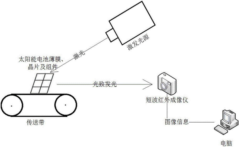
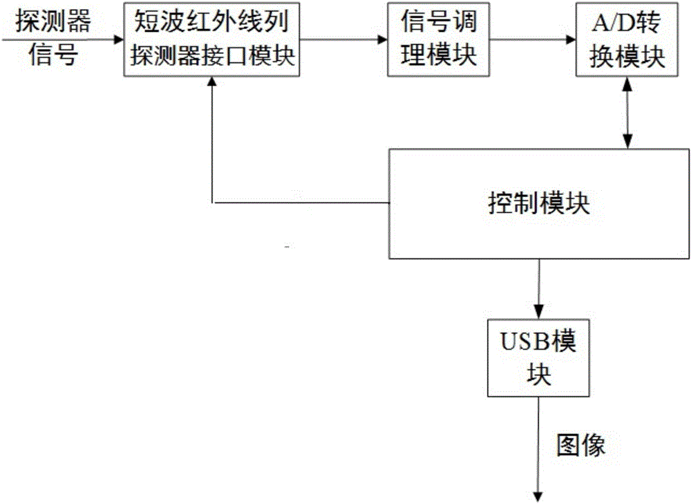
[0040] Solar cell photoluminescence high-speed detection system based on short-wave infrared imager, including 15W 808nm continuous laser, conveyor belt, computer, also includes line scan InGaAs short-wave infrared imager, line scan InGaAs short-wave infrared imager connected to computer, such as figure 1 shown. The line-scanning InGaAs short-wave infrared imager receives the fluorescent signal emitted by the 10cm×5cm copper indium gallium selenide material solar cell film for imaging to obtain photoluminescence images.
[0041] For most solar cells, when the laser wavelength of the excitation light source is less than 900nm, the photoluminescence condition is satisfied. In this embodiment, a 15W 808nm continuous laser is selected as the excitation light source. Place the 15W 808nm laser at a distance of about 70cm from the solar cell film, wafer and small components at a 45° angle to its normal direction, and aim at the solar cell film, wafer and small components, and slowly ...
Embodiment 2
[0052] The operating method of the solar cell photoluminescence high-speed detection system based on the short-wave infrared imager described in embodiment 1, the specific steps include:
[0053] (1) Place the solar cell film, wafer and component on the conveying scanning device, place the excitation light source device at a distance of 70 cm from the solar cell film, wafer and component, and place the solar cell film, wafer and component together The component normal is 45° and aligned with the solar cell film, wafer and component;
[0054] (2) The excitation light source device emits laser light to the surface of the solar cell thin film, wafer and component, and excites the solar cell thin film, wafer and component to emit fluorescent signals;
[0055] (3) The short-wave infrared imager is placed on the normal direction 1m away from the solar cell film, wafer and component, receives the fluorescent signal sent by the solar cell film, chip and component for imaging, and obta...
PUM
 Abstract
Description
Claims
Application Information
 - R&D Engineer
- R&D Manager
- IP Professional
- Industry Leading Data Capabilities
- Powerful AI technology
- Patent DNA Extraction
Browse by: Latest US Patents, China's latest patents, Technical Efficacy Thesaurus, Application Domain, Technology Topic, Popular Technical Reports.
© 2024 PatSnap. All rights reserved.Legal|Privacy policy|Modern Slavery Act Transparency Statement|Sitemap|About US| Contact US: help@patsnap.com


