
Eureka
For R&D, Eureka makes reading and utilizing patents & technical documents easy.
Eureka AIR
Designed for self-driven R&D workflows. Generate viable solutions, solve complex R&D challenges, empower your innovation with AI.

Eureka Materials
Designed for material experts only. Revolutionize your material R&D, from search, analyze, to developing new materials.

TechResearch
Generate reliable direction feasibility study reports for your R&D in just a few steps.

TechSeek
Discover and master advanced knowledge NOW. Basics, ideas, possibilities, all at once.

TechMind
As an expert in R&D Theories, TechMind can generates customized viable solutions instantly.

TechRisk
Analyze your overall solution with one click, know your potential R&D risks in advance.

TechMonitor
Get weekly tech updates, stay abreast of the latest tech innovations and key insights.
Semiconductor device and manufacturing method thereof
A manufacturing method and semiconductor technology, applied in semiconductor/solid-state device manufacturing, semiconductor devices, electric solid-state devices, etc., can solve problems such as integrated circuit reliability degradation, MOS device gate damage, and integrated circuit application performance degradation
- Summary
- Abstract
- Description
- Claims
- Application Information
AI Technical Summary
Problems solved by technology
Method used
Image


Examples
Embodiment 1
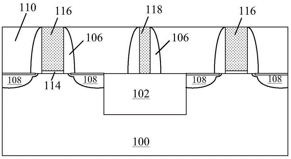
[0053] In this embodiment, the resistive structure and the gate of the MOS device have the same material and structure, are formed in the same step, and have good compatibility with the gate-last process.
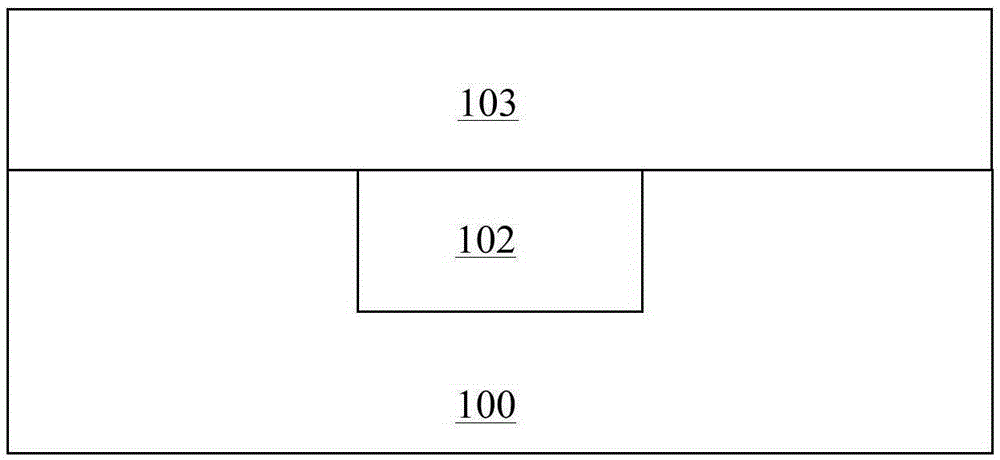
[0054] Step S101, providing a semiconductor substrate, refer to figure 2 shown.
[0055]In the embodiment of the present invention, the semiconductor substrate 200 may be a Si substrate, a Ge substrate, a SiGe substrate, SOI (Silicon On Insulator, Silicon On Insulator) or GOI (Germanium On Insulator, Germanium On Insulator) and the like. In other embodiments, the semiconductor substrate may also be a substrate including other elemental semiconductors or compound semiconductors, such as GaAs, InP or SiC, etc., or a stacked structure, such as Si / SiGe, etc., or other epitaxial Structures, such as SGOI (silicon germanium on insulator), etc.
[0056] In this embodiment, the semiconductor substrate 100 is a silicon substrate.
[0057] Step S102, forming an isolation 102 in th...
Embodiment 2
[0076] In this embodiment, only the parts that are different from the first embodiment are described, and the same parts are regarded as the same as the first embodiment, and will not be described again. In this embodiment, the resistor structure is integrated in a gate-first process.
[0077] In step S201 and step S202, provide semiconductor substrate 200, and form isolation 202 in semiconductor substrate, refer to Figure 9 shown.
[0078] Same as step S101 and step 102 in the first embodiment.
[0079] In step S203, a MOS device is formed on the semiconductor substrate 200, referring to Figure 10 shown.
[0080] In this step, a conventional gate-front manufacturing process can be used to form a MOS device. In this embodiment, specifically, first, gate dielectric material and gate material are deposited, then patterned to form gate dielectric layer 203 and gate 204, and then spacer 206 and source and drain regions 208 are formed , further perform silicide on the source...
Embodiment 3
[0090] In this embodiment, only the parts that are different from the first embodiment are described, and the same parts are regarded as the same as the first embodiment, and will not be described again. In this embodiment, the resistance structure is formed at the same time as the gate is formed in the gate-front process, and the process is simpler and easier.
[0091] Step S301, providing a semiconductor substrate, refer to figure 2 shown.
[0092]In the embodiment of the present invention, the semiconductor substrate 200 may be a Si substrate, a Ge substrate, a SiGe substrate, SOI (Silicon On Insulator, Silicon On Insulator) or GOI (Germanium On Insulator, Germanium On Insulator) and the like. In other embodiments, the semiconductor substrate may also be a substrate including other elemental semiconductors or compound semiconductors, such as GaAs, InP or SiC, etc., or a stacked structure, such as Si / SiGe, etc., or other epitaxial Structures, such as SGOI (silicon germani...
PUM
 Abstract
Description
Claims
Application Information
 - R&D Engineer
- R&D Manager
- IP Professional
- Industry Leading Data Capabilities
- Powerful AI technology
- Patent DNA Extraction
Browse by: Latest US Patents, China's latest patents, Technical Efficacy Thesaurus, Application Domain, Technology Topic, Popular Technical Reports.
© 2024 PatSnap. All rights reserved.Legal|Privacy policy|Modern Slavery Act Transparency Statement|Sitemap|About US| Contact US: help@patsnap.com