Full-automatic PCB (printed circuit board) making system and method based on Internet of Things

A technology of PCB board and PCB circuit board, which is applied in the field of fully automatic PCB board making system, can solve the problems such as the inability to make PCB circuit boards, and achieve the effect of efficient and fast production process

Pending Publication Date: 2017-03-29
HUBEI UNIV OF EDUCATION
View PDF7 Cites 6 Cited by
  • Summary
  • Abstract
  • Description
  • Claims
  • Application Information

AI Technical Summary

Problems solved by technology

The patent of the special laser printer for PCB circuit board production (CN 203418825 U) is for printing on PCB circuit boards, but cannot make PCB circuit boards

Method used


Image

  • Full-automatic PCB (printed circuit board) making system and method based on Internet of Things
  • Full-automatic PCB (printed circuit board) making system and method based on Internet of Things
  • Full-automatic PCB (printed circuit board) making system and method based on Internet of Things

Examples


Embodiment Construction

[0035] The present invention will be further described below in conjunction with the accompanying drawings and specific embodiments.

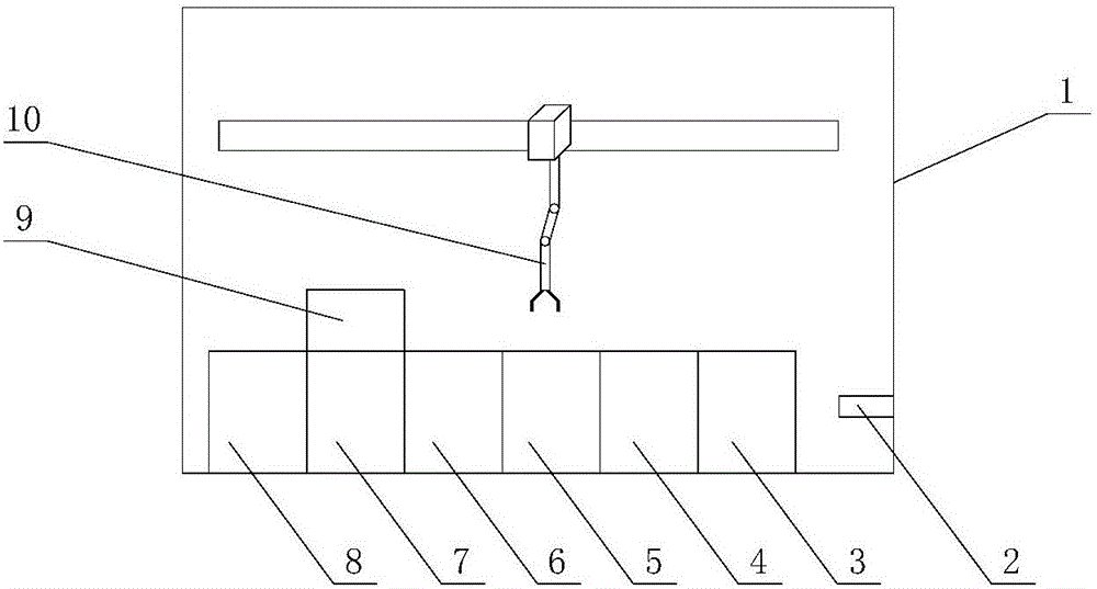
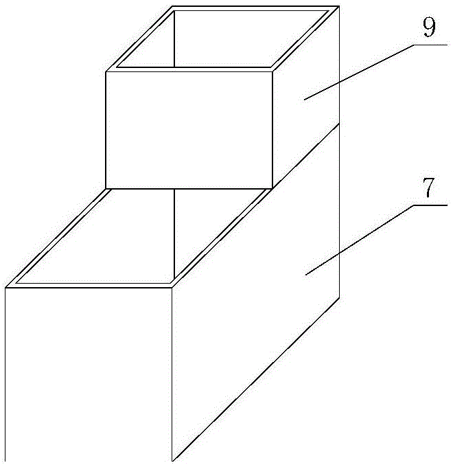
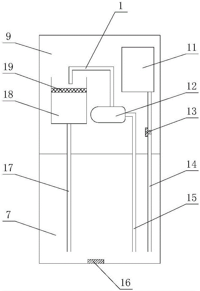
[0036] Figure 1 to Figure 9 It schematically shows the structure of a fully automatic PCB manufacturing system according to an embodiment of the present invention.

[0037] Such as Figure 1 to Figure 9 As shown, a fully automatic PCB system and method based on the Internet of Things is characterized in that it includes a housing, a PCB circuit board laser printer, a corrosion tank, a cleaning tank device, a polishing tank device, a multi-joint manipulator and a control module; The corrosion tank, the cleaning tank device, the polishing tank device and the multi-joint manipulator are arranged on the housing, and the PCB circuit board laser printer is used to print a PCB circuit board with a protective layer;

[0038] The control module generates a control signal, and sends the control signal to the multi-joint manipulator, and the multi-join...


PUM


Abstract

The invention relates to a full-automatic PCB (printed circuit board) making system and method based on Internet of Things. The system is characterized by comprising a shell, a PCB laser printer, an etching trench, a rinsing trench device, a polishing trench device, a multi-joint manipulator and a control module, wherein the etching trench, the rinsing trench device, the polishing trench device and the multi-joint manipulator are arranged on the shell; the PCB laser printer is used for printing a PCB; the control module generates a control signal and sends the control signal to the multi-joint manipulator; the multi-joint manipulator is used for grabbing an external PCB, and placing the circuit board in the etching trench, the rinsing trench device or the polishing trench device. Through the interaction of the PCB laser printer, the etching trench, the rinsing trench device, the polishing trench device, the multi-joint manipulator and the control module disclosed by the invention, a complete PCB is manufactured; the manufacturing process is efficient and fast and can be used for small-scale production in schools or laboratories.

Description

technical field [0001] The invention relates to a fully automatic PCB board manufacturing system and method based on the Internet of Things. Background technique [0002] PCB circuit board, also known as printed circuit board, is the provider of electrical connection for electronic components. The patent of the special laser printer (CN 203418825 U) for making PCB circuit boards is for printing on PCB circuit boards, but cannot make PCB circuit boards. Contents of the invention [0003] In view of the above, the object of the present invention is to provide a fully automatic PCB system and method based on the Internet of Things. It utilizes a PCB circuit board laser printer to print out the PCB circuit board, and through the corrosion tank, cleaning tank device and polishing tank device After processing, a complete PCB circuit board is produced. [0004] In order to achieve the purpose of the present invention, the technical solution adopted is: a fully automatic PCB sys...

Claims


Application Information

Patent Timeline
Patent Type & Authority Applications(China)
IPC IPC(8): H05K3/00
CPCH05K3/00
Inventor 肖鹏程王骐陈磊石健攀付家衡杨志杭
Owner HUBEI UNIV OF EDUCATION
Why Eureka
Try Eureka