Supercharge Your Innovation With Domain-Expert AI Agents!

CMOS nonvolatile memory unit circuit

A non-volatile memory, unit circuit technology, applied in the field of integrated circuits, can solve the problems of data read reliability, data write or erase time increase, etc., to avoid data write speed, reduce area, shorten The effect of the production cycle

Active Publication Date: 2017-04-19
SHANGYANG RFID TECH YANGZHOU +1
View PDF4 Cites 0 Cited by
  • Summary
  • Abstract
  • Description
  • Claims
  • Application Information

AI Technical Summary

Problems solved by technology

On the other hand, this kind of memory usually uses a single voltage for electronic erasing and electron injection, which takes longer time during the electronic erasing operation, resulting in an increase in data writing or erasing time
In addition, memory usually uses the same transistor for electronic tunneling and data reading. As the working time increases, electronic tunneling can lead to changes in the threshold voltage of the transistor, which affects the reliability of later data reading.

Method used


Image

  • CMOS nonvolatile memory unit circuit
  • CMOS nonvolatile memory unit circuit

Examples


Embodiment Construction

[0024] In order to make the object, technical solution and advantages of the present invention clearer, the present invention will be described in further detail below in conjunction with specific embodiments and with reference to the accompanying drawings.

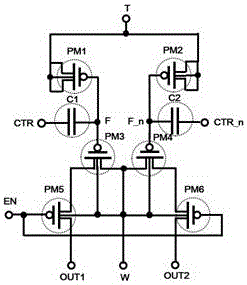
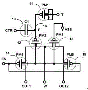
[0025] figure 2 It is the circuit diagram of the non-volatile storage unit circuit proposed by the present invention. The circuit is realized by 0.18 μm single-layer polysilicon CMOS technology. The PMOS tube in the figure is realized by 3.3V input and output transistors, and the thickness of its gate oxide is about 7nm. The circuit has four signal input ports: CTR, T, W, EN and two signal output ports: OUT 1 and OUT 2 .

[0026] The circuit consists of five PMOS transistors PM 1 11~PM 5 15 and a capacitor C 1 10 composition;

[0027] Two PMOS transistors PM 1 11 and PM 2 12 gate and capacitor C 1 One port of 10 is connected together to form a floating charge storage node F 16;

[0028] Capacitance C 1 Th...


PUM


Abstract

The invention discloses a CMOS nonvolatile memory unit circuit having four signal input ports which respectively are CTR, T, W and EN, and two signal output ports which respectively are OUT1 and OUT2. The circuit is composed of five PMOS transistors PM1-PM5 and a capacitor C1. The grids of the transistors PM1 and PM2 are connected with a port of the capacitor C1 to form a floating storage charge node; the grid of the transistor PM3 is earthed, and serve as a reference transistor when data is read; and the transistors PM4 and PM5 are used as switches for controlling data output of the memory unit. The circuit has the characteristics of simple technological process, shorter processing time and lower cost; in addition, the electron tunneling transistor of the circuit and the data read transistor are achieved by the different transistors, influence of electron injection and erasing operations on reading performance of the memory unit is avoided, an external electric field used during electron erasing is stronger than that used during electron injection, and a data writing speed is improved.

Description

technical field [0001] The invention relates to the technical field of integrated circuits, in particular to a CMOS nonvolatile memory unit circuit, which can be realized based on a single-layer polysilicon CMOS process, and is especially suitable for use in ultra-low power consumption and low-cost embedded nonvolatile memory chips. [0002] technical background [0003] Non-volatile memory based on single-layer polysilicon CMOS technology can realize reliable data storage after power failure. Compared with EEPROM and FLASH memory, its advantages are simple process flow, short production cycle, and low production cost. Applications that require small-capacity storage after power-on have good application prospects, such as the calibration of analog / RF circuits and the storage of key circuit parameters. The non-volatile memory realized by single-layer polysilicon CMOS technology can avoid the use of small-capacity EEPROM or FLASH memory, which will lead to increased product pro...

Claims


Application Information

Patent Timeline
Patent Type & Authority Applications(China)
IPC IPC(8): G11C16/10
CPCG11C16/10Y02D10/00
Inventor 王开友吴南健冯鹏李贵柯邓元明伯林
Owner SHANGYANG RFID TECH YANGZHOU
Features
  • R&D
  • Intellectual Property
  • Life Sciences
  • Materials
  • Tech Scout
  • Unparalleled Data Quality
  • Higher Quality Content
  • 60% Fewer Hallucinations
Learn More