Solid power semiconductor field effect transistor structure

A technology of field effect transistors and power semiconductors, which is applied in the field of solid power semiconductor field effect transistor structures, can solve problems such as device failures and cannot be eliminated, and achieve the effect of enhanced robustness

Active Publication Date: 2017-04-19
安建科技(深圳)有限公司
View PDF3 Cites 4 Cited by
  • Summary
  • Abstract
  • Description
  • Claims
  • Application Information

AI Technical Summary

Problems solved by technology

At present, VDMOS has been widely used in electronic systems, however, there is always a parasitic bipolar junction transistor (i.e., a triode) composed of an n+ source region 111, a p-type body region 113 and an n-drift region 114 in this structure, and Activation of this parasitic transistor can lead to device failure under transient conditions that typically include (but are not limited to) avalanche operation, reverse recovery of the body diode, and cosmic radiation-induced single-event events, and these conditions typically cause Encountered in the application, since the parasitic triode exists in all VDMOS structures, the related faults can only be suppressed but not eliminated

Method used


Image

  • Solid power semiconductor field effect transistor structure
  • Solid power semiconductor field effect transistor structure
  • Solid power semiconductor field effect transistor structure

Examples


Embodiment 1

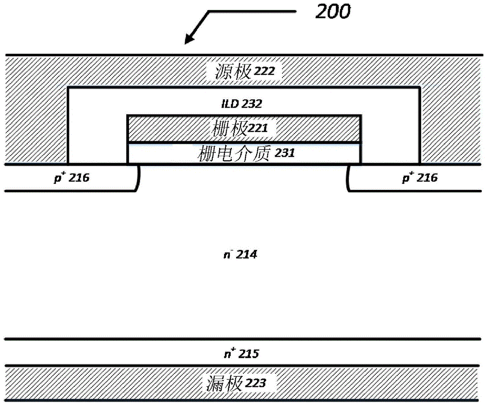
[0035] Embodiment 1: Please refer to the attached figure 2 , in this embodiment, the bottom of the field effect transistor body 200 is the drain 223, and the top of the drain 223 is provided with n + drain region 215, the n + On top of the drain region 215 is provided n - Drift zone 214, n - The upper surface portion of the drift region 214 is provided with p + source region 216, covering n - part of the upper surface of the drift region 214, at n - Drift Zone 214 and p + A gate dielectric 231 is provided on top of the source region 216, and the gate dielectric 231 covers the n - above the drift zone 214 and cover a part of p + The top of the source region 216 and the top of the gate dielectric 231 are provided with a gate 221, and the top of the gate 221 is provided with an interlayer dielectric 232 (i.e. ILD). The interlayer dielectric 232 covers the top of the gate 221 and is connected with p + The upper surface of the source region 216 is in contact, the top of t...

Embodiment 2

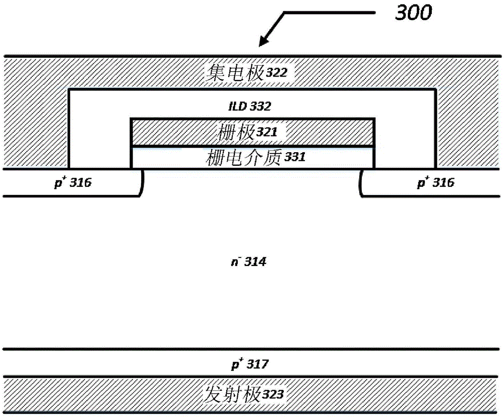
[0038] Embodiment two: Please refer to the attached image 3 , this embodiment is a gate-controlled PNP bipolar junction transistor (triode). The bottommost part of the field effect transistor body 300 is the emitter 323, and the top of the emitter 323 is provided with a p + Launch Area 317, at p + On top of the emission area 317 is provided n - Base 314, n - The upper surface portion of the base region 314 is provided with p + collector area 316, covering n - part of the upper surface of the base region 314, the n - Base 314 and p + A gate dielectric 331 is provided on top of the collector region 316, and the gate dielectric 331 covers the n - over the base region 314 and cover part of the p + The top of the collector region 316 and the top of the gate dielectric 331 are provided with a gate 321, and the top of the gate 321 is provided with an interlayer dielectric 332 (ie ILD). In this embodiment, the cross section of the interlayer dielectric 332 is in the shape of ...

Embodiment 3

[0041] Embodiment three: Please refer to the attached Figure 4 , the structure of this embodiment is similar to that of Embodiment 1. In this embodiment, in n - A trench gate is disposed in the drift region 414 , and the gate dielectric 431 and the gate 421 are located in the trench. The trench gate structure can lead to reduced cell pitch and thus reduced on-resistance of the device.


PUM


Abstract

The invention discloses a solid power semiconductor field effect transistor structure. Through special design, no any parasitic triode exists in the solid power semiconductor field effect transistor structure, thereby solving the problem that a device fails due to secondary breakdown or latching under transient conditions. The firmness of the device is enhanced.

Description

technical field [0001] The present invention discloses a structure of a power semiconductor device, and in particular relates to a solid power semiconductor field effect transistor structure. Background technique [0002] Power semiconductor switching devices are widely used in power electronic systems, such as switching power supplies and motor drives, etc. These applications usually require that these devices should have high robustness. Please see attached figure 1 , figure 1 Shown in is a cross-section of a prior art power semiconductor device structure, figure 1 Devices with a medium structure are commonly referred to as vertical double-diffused metal-oxide-semiconductor field-effect transistors (VDMOS). The bottommost part of the field effect transistor body 100 is the drain 123, and the top of the drain 123 is provided with n + The drain region 115, namely the heavily doped n-type drain region, is in the n + On top of the drain region 115 is provided n - Drift r...

Claims


Application Information

Patent Timeline
Patent Type & Authority Applications(China)
IPC IPC(8): H01L29/78H01L21/336H01L29/06
CPCH01L29/0603H01L29/0684H01L29/66734H01L29/7802H01L29/7813
Inventor 周贤达廖慧仪单建安
Owner 安建科技(深圳)有限公司
Why Eureka
Try Eureka