Structure and method for forming optical splitting lens

A spectroscopic lens and optical technology, applied in the direction of optics, lenses, optical components, etc., can solve the problems of incompatibility of integrated circuit manufacturing processes, and achieve the effect of convenient formation

Active Publication Date: 2017-04-26
SHANGHAI INTEGRATED CIRCUIT RES & DEV CENT
View PDF4 Cites 8 Cited by
  • Summary
  • Abstract
  • Description
  • Claims
  • Application Information

AI Technical Summary

Problems solved by technology

At present, optical splitting lenses are formed during packaging, which can only reflect specific wavelengths of light, and are not compatible with existing integrated circuit manufacturing processes

Method used


Image

  • Structure and method for forming optical splitting lens
  • Structure and method for forming optical splitting lens
  • Structure and method for forming optical splitting lens

Examples


Embodiment Construction

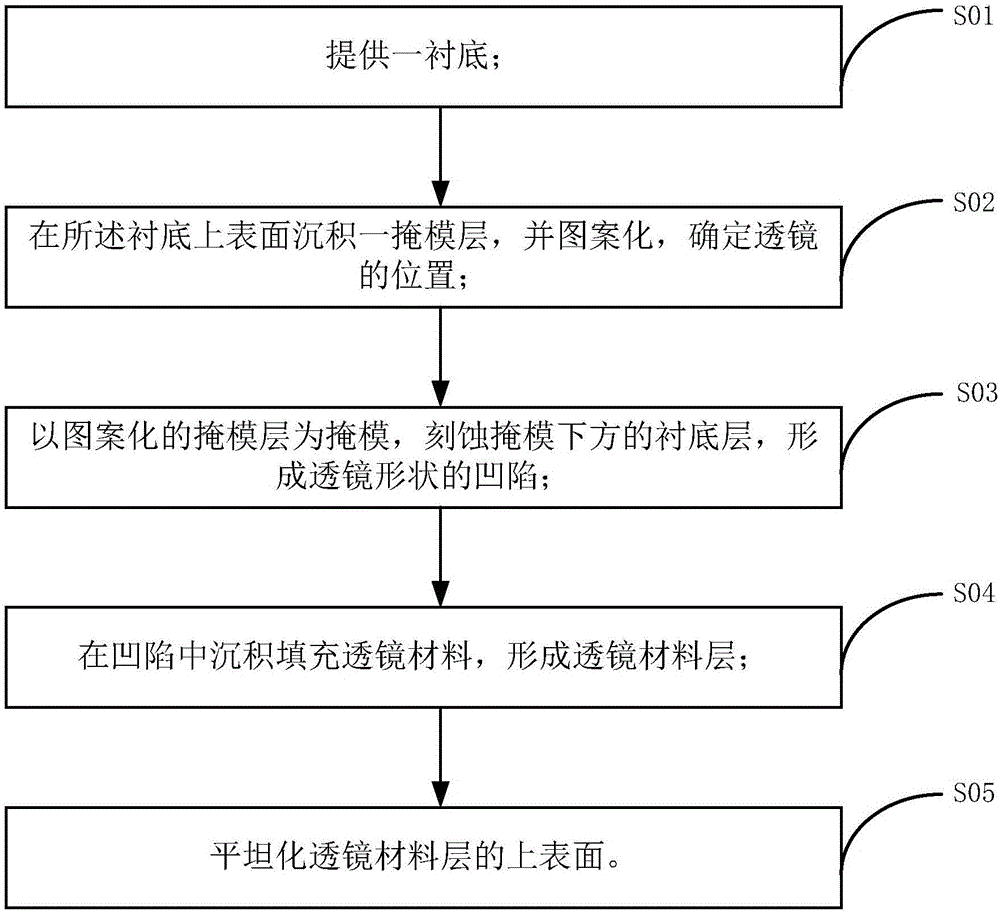
[0029] The present invention will be described in further detail below in conjunction with specific embodiments.

[0030] It should be noted that, in the following specific embodiments, when describing the embodiments of the present invention in detail, in order to clearly show the structure of the present invention for the convenience of description, the structures in the drawings are not drawn according to the general scale, and are drawn Partial magnification, deformation and simplification are included, therefore, it should be avoided to be interpreted as a limitation of the present invention.

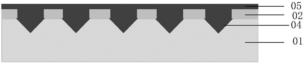
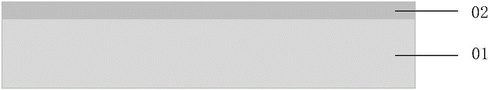
[0031] Please refer to figure 1 , figure 1 It is a structural schematic diagram of an optical beam splitting lens of the present invention. As shown in the figure, the structure of an optical spectroscopic lens provided by the present invention includes a substrate layer 01, a mask layer 02, and a lens material layer 05 from bottom to top. The substrate layer 01 contains a lens-s...


PUM


Abstract

The present invention provides a structure for forming an optical splitting lens. Through changing the material of a lens material layer and the shape of a lens, the light splitting characteristics of different light wave ranges can be obtained, and the requirement from ultraviolet light to infrared light is satisfied. The invention also provides a method for forming an optical splitting lens, through forming different recesses with lens shapes by using crystal orientation etching in a substrate and depositing lens materials in the recesses to form lenses, various optical splitting lenses can be formed conveniently, and the method can be fully compatible with an existing integrated circuit manufacturing process.

Description

technical field [0001] The invention belongs to the technical field of semiconductor integrated circuit manufacturing technology, and in particular relates to a structure and method for forming an optical beam splitting lens. Background technique [0002] Silicon-based optical sensors (CCD / CIS, charge-coupled device / CMOS image sensor) are the mainstream of optical image sensors. In order to obtain a color image, an optical splitter lens is required to split the light. At present, optical splitter lenses are all formed during packaging, can only reflect light of a specific wavelength, and are not compatible with existing integrated circuit manufacturing processes. As the size of the sensor continues to shrink, the size of the lens must also shrink accordingly, which puts forward higher requirements for materials and processes. Contents of the invention [0003] The purpose of the present invention is to overcome the above-mentioned defects, and proposes a structure and me...

Claims


Application Information

Patent Timeline
Patent Type & Authority Applications(China)
IPC IPC(8): G02B3/00H01L27/146
CPCG02B3/0018G02B3/0068H01L27/14627
Inventor 储佳
Owner SHANGHAI INTEGRATED CIRCUIT RES & DEV CENT
Why Eureka
Try Eureka