

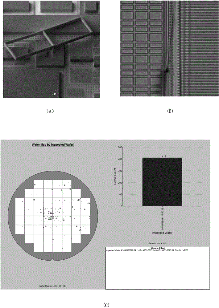
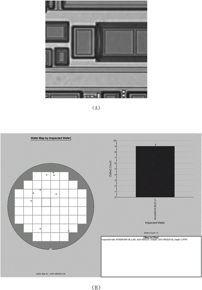
Method for preventing peeling of photoresist
A photoresist and ultraviolet light technology, applied in the direction of optics, optomechanical equipment, photoplate making process of pattern surface, etc., can solve the problems of peeling, colloid shrinkage, stress generation, etc., and achieve the effect of avoiding peeling and good graphics
- Summary
- Abstract
- Description
- Claims
- Application Information
AI Technical Summary
Problems solved by technology
Method used
Image

Examples
Embodiment Construction
[0018] In order to have a more specific understanding of the technical content, characteristics and effects of the present invention, the technical solution of the present invention will be further described in detail in conjunction with the accompanying drawings and specific embodiments.
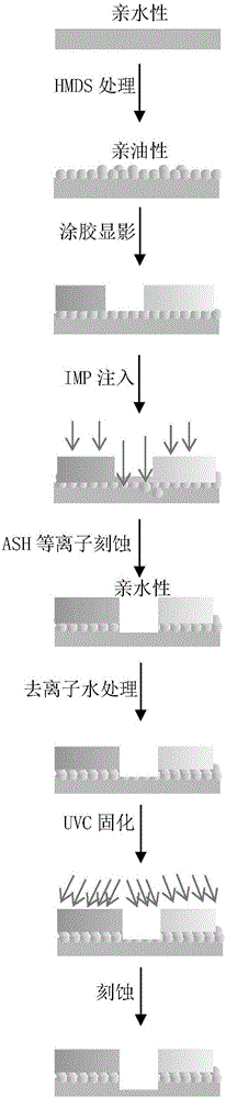
[0019] The method for preventing the photoresist peeling of the present embodiment, its specific processing process flow is as follows (see figure 2 ):
[0020] Step 1, pre-treat the silicon substrate with the oxide film with HMDS (hexamethyldisilazane) to change the hydrophilicity of the surface of the silicon substrate to lipophilicity to facilitate the adhesion of the photoresist.
[0021] Step 2, spin-coating and baking the photoresist.
[0022] Step 3, using a mask to expose and develop to form the desired etching pattern.
[0023] Step 4, performing an ion implantation (IMP) process.
[0024] In step 5, ASH plasma (plasma) etching is used to process the surface of the silicon subs...
PUM
 Abstract
Description
Claims
Application Information