LED epitaxial structure
An epitaxial structure, hole blocking layer technology, applied in electrical components, circuits, semiconductor devices, etc., can solve the problems of neglect, leakage, and hole leakage intensified, and achieve the effect of improving luminous efficiency
- Summary
- Abstract
- Description
- Claims
- Application Information
AI Technical Summary
Problems solved by technology
Method used
Image
Examples
Embodiment 1
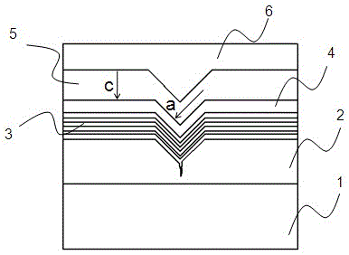
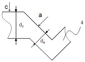
[0028] see figure 1 with figure 2 , for an LED epitaxial structure implemented in the present invention, it includes from bottom to top: a substrate 1, a first conductivity type semiconductor layer 2, a superlattice layer 3 with V-shaped pits, a hole blocking layer 4, and an active region The light emitting layer 5 and the second conductivity type semiconductor layer 6 . The first conductive type semiconductor layer 2 includes N-GaN, or U-GaN and N-GaN, and the second conductive type semiconductor layer 2 includes at least P-GaN.
[0029] During the growth process of growing LEDs, many defects such as dislocations are generated, and some dislocations extend along the growth direction and penetrate the entire LED structure. When the dislocation enters the superlattice layer 3, by controlling the growth conditions of the superlattice layer 3, at the penetrating dislocation position, the V-shaped pit nucleates and grows to release the stress. The material In of the superlattic...
Embodiment 2
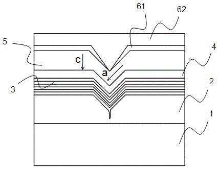
[0034] see image 3 The difference between this embodiment and Embodiment 1 is that the first conductivity type semiconductor layer 2 includes an N-GaN layer, or includes a U-GaN layer and an N-GaN layer, and the second conductivity type semiconductor layer 6 includes an electron blocking layer 61 and P-GaN 62. On the basis of Embodiment 1, an electron blocking layer 61 is provided on the second conductivity type semiconductor layer 6 to prevent electrons from leaking from the light emitting layer 5 in the active region to the P-GaN 62 and reduce the luminous efficiency. The material of the electron blocking layer 61 can be a single-layer AlGaN structure or an AlGaN / GaN superlattice structure or an AlGaN / InGaN superlattice structure or an AlGaN / InGaN / GaN superlattice structure, and can be partially doped with Mg or fully doped with Mg or non- doping.
Embodiment 3
[0036] see Figure 4The difference between this embodiment and Embodiment 1 is that the second conductivity type semiconductor layer 6 includes a hole injection layer 63 and a P-GaN 62 . In the V-shaped pit of the light-emitting layer 5 in the active area, a hole injection layer 63 is set to promote holes from P-GaN 62 to enter the light-emitting layer 5 in the active area, thereby improving the light coupling efficiency, wherein the hole injection layer 63 can be set as The hexagonal pyramid type can also fill the active light-emitting layer 5, and the material of the hole injection layer 63 can be Mg-doped GaN layer or InxGa1-xN (0<x ≤ 1) or P-GaN / U-GaN periodic structure .
PUM
| Property | Measurement | Unit |
|---|---|---|
| Thickness | aaaaa | aaaaa |
| Thickness | aaaaa | aaaaa |
Abstract
Description
Claims
Application Information


