Flexible OLED display and manufacturing method thereof

A manufacturing method and display technology, applied in semiconductor/solid-state device manufacturing, electric solid-state devices, semiconductor devices, etc., can solve the problem of affecting the packaging effect of flexible OLED displays, increasing light loss of flexible OLED displays, increasing edge stress of packaging structures, etc. problem, achieve the effect of improving the light extraction ability, reducing the water vapor transmission rate, and reducing the edge stress

Active Publication Date: 2017-05-10
WUHAN CHINA STAR OPTOELECTRONICS TECH CO LTD
View PDF6 Cites 11 Cited by
  • Summary
  • Abstract
  • Description
  • Claims
  • Application Information

AI Technical Summary

Problems solved by technology

Due to the slow deposition rate of ALD, PECVD is often used to deposit the barrier layer. However, due to technical limitations, the barrier layer produced by PECVD mostly has needle-shaped holes and has limited water vapor barrier capability (water vapor transmission rate of 10 -4 g/(m 2 24h))
In order to achieve a water vapor barrier packaging effect comparable to that of glass packaging (water vapor transmission rate-6 g/(m 2 24h)), the common practice is to deposit more layers of packaging film, and set the size of the barrier layer larger than the size of the buffer layer below it, so that the barrier layer

Method used


Image

  • Flexible OLED display and manufacturing method thereof
  • Flexible OLED display and manufacturing method thereof
  • Flexible OLED display and manufacturing method thereof

Examples


Example

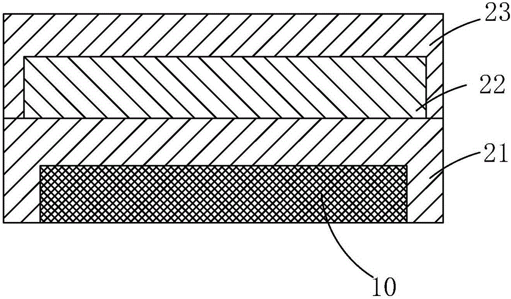
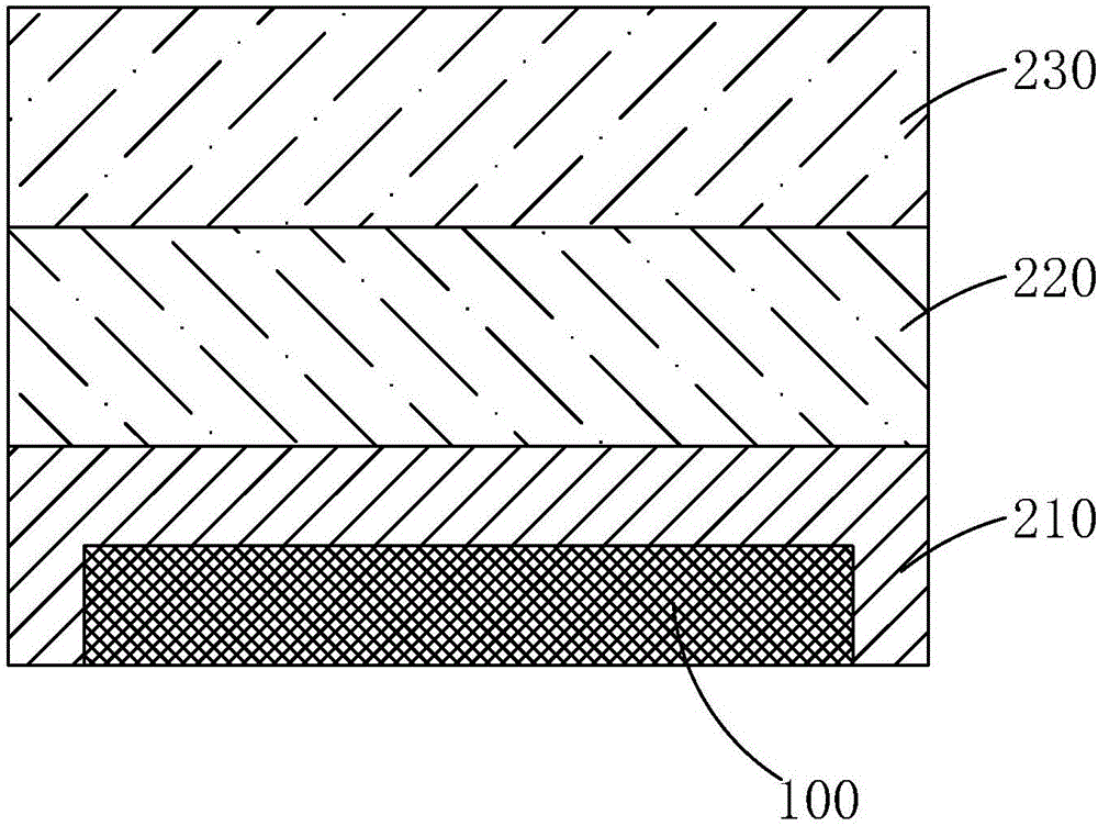
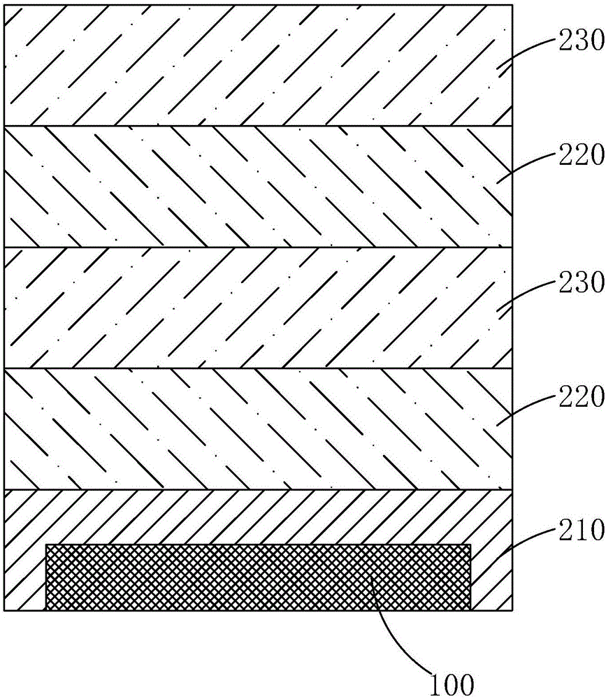
[0051] The present invention provides a flexible OLED display, please refer to figure 2 , Is the first embodiment of the flexible OLED display of the present invention, and includes a flexible substrate (not shown), an OLED device 100 provided on the flexible substrate, a barrier layer 210 covering the upper surface and sides of the OLED device 100, A water absorption buffer layer 220 provided on the barrier layer 210, and a light extraction enhancement buffer layer 230 provided on the water absorption buffer layer 220;

[0052] The water-absorbing buffer layer 220 includes a first organic material and water-absorbing particles doped in the first organic material;

[0053] The light extraction enhancement buffer layer 230 includes a second organic material and refractive particles doped in the second organic material;

[0054] The size of the area covered by the barrier layer 210, the water absorption buffer layer 220, and the light extraction enhancement buffer layer 230 are the sa...


PUM

PropertyMeasurementUnit
Thicknessaaaaaaaaaa
Thicknessaaaaaaaaaa

Abstract

The invention provides a flexible OLED display and a manufacturing method thereof. The flexible OLED display comprises an OLED device arranged on a flexible substrate, a barrier layer covering the OLED device, a water-absorbing buffer layer arranged on the barrier layer, and a light-extraction enhanced buffer layer arranged on the water-absorbing buffer layer, wherein the water-absorbing buffer layer is doped with water-absorbing particles; the light-extraction enhanced buffer layer is doped with refraction particles; and the areas covered by the barrier layer, the water-absorbing buffer layer and the light-extraction enhanced buffer layer are the same in size and are used for packaging the OLED device as a packaging structure in common. Compared with the prior art, the flexible OLED display has the advantages that the water vapor transmission rate of the water-absorbing buffer layer manufactured by an organic material is reduced, the utilization rate of the water-absorbing buffer layer is improved and the packaging effect of the flexible OLED display can be greatly improved, so that the service life of the OLED display is prolonged; and meanwhile, the light extraction ability of the flexible OLED display is improved and the quality and the reliability of a product are improved.

Description

technical field [0001] The invention relates to the field of display technology, in particular to a flexible OLED display and a manufacturing method thereof. Background technique [0002] Organic light-emitting diode (Organic Light-Emitting Diode, OLED) display, also known as organic electroluminescent display, is a new type of flat panel display device, due to its simple preparation process, low cost, low power consumption, high luminance, Wide range of working temperature, light and thin size, fast response speed, easy to realize color display and large-screen display, easy to realize matching with integrated circuit driver, easy to realize flexible display, etc., so it has broad application prospects. [0003] According to the driving method, OLED can be divided into two categories: passive matrix OLED (Passive Matrix OLED, PMOLED) and active matrix OLED (Active Matrix OLED, AMOLED), namely direct addressing and thin film transistor (ThinFilm Transistor, TFT) matrix Two ...

Claims


Application Information

Patent Timeline
IPC IPC(8): H01L51/52H01L51/56H01L51/00
CPCH10K77/111H10K50/846H10K50/85H10K50/8426H10K71/00Y02E10/549Y02P70/50
Inventor 张明
Owner WUHAN CHINA STAR OPTOELECTRONICS TECH CO LTD
Why Eureka
Try Eureka