FIR filter bank and filtering method
A filter bank and controller technology, applied in impedance networks, digital technology networks, electrical components, etc., can solve the problem of inability to provide filter bank reconfigurability, lack of single filter reconfigurability, and low resource utilization. And other issues
- Summary
- Abstract
- Description
- Claims
- Application Information
AI Technical Summary
Problems solved by technology
Method used
Image

Examples
Embodiment 1
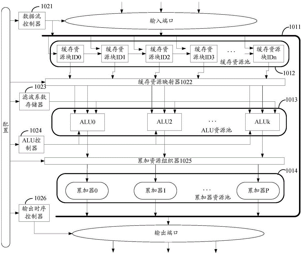
[0041] The basic idea of the technical solution of the embodiment of the present invention is to consider all the hardware resources of the filter in a unified manner, so that the filtering resources can be reorganized according to different application scenarios, thereby forming different filter bank structures, and realizing the filter Group reconfigurability.
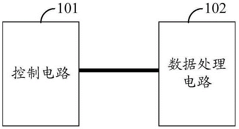
[0042] see figure 1 , which shows the structure of a FIR filter bank 10 proposed by the embodiment of the present invention. Such as figure 1As shown, the FIR filter bank 10 includes two components: a data processing circuit 101 and a control circuit 102, and these two components are coupled to each other. Understandably, since this embodiment is an example description of the structure of the FIR filter bank 10, therefore, for the external circuits and electrical components related to the FIR filter bank 10, this embodiment does not specifically describe them in detail, and those skilled in the art The relevant ...
Embodiment 2
[0061] see Figure 6 , which shows a filtering method applied to the FIR filter bank described in the foregoing embodiment, the specific structure of the FIR filter bank is as described in the foregoing embodiment, and will not be repeated here, and the filtering method may include:
[0062] S601: After the input port receives the input data, transmit the input data to the data flow bus array;
[0063] Specifically, transmitting the input data to the data stream bus array may include:
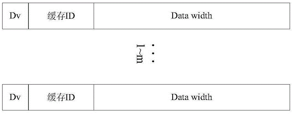
[0064] When the input data is transmitted to the data stream bus in the data stream bus array, the ID is correspondingly identified, and the corresponding identification bit dv used to represent the data as new data is set to valid.
[0065] S602: The cache resource blocks in the cache resource pool receive the data transmitted by the data stream bus array according to the control of the data flow controller, and control them through the data flow controller according to the filter order, numb...
Embodiment 3
[0076] Taking two series filters as an example, set the first-stage filter to have 12 coefficients with even symmetry, 2 times decimation, and 3 times the input multiplexing ratio; the second-stage filter has 47 coefficients with odd symmetry, 2 times decimation, 6 times the input multiplexing ratio. Based on the FIR filter bank and filtering method described in the foregoing embodiments, the specific implementation process is as follows:
[0077] Set the first-stage filter to occupy ID0 and ID1 two cache resource blocks, the cache cascade switch of cache resource block ID0 is set to be connected to the data flow bus array, and the input data of the register group of cache resource block ID0 is controlled by the data flow bus Provided by the array; the cache cascade switch of the cache resource block ID1 is set to be connected to the previous cache resource block ID0, and the input data of the register group of the cache resource block ID1 is provided by the cache resource blo...
PUM
 Abstract
Description
Claims
Application Information