A charge pump and electronic equipment including the same

A technology of electronic equipment and charge pump, applied in the field of charge pump, can solve the problem of high power consumption of electronic equipment, and achieve the effect of slow response

Active Publication Date: 2020-02-14
CAPITAL MICROELECTRONICS
View PDF6 Cites 0 Cited by
  • Summary
  • Abstract
  • Description
  • Claims
  • Application Information

AI Technical Summary

Problems solved by technology

However, due to a certain degree of leakage current in the MOS transistor, there is a certain leakage current in the charge pump, resulting in high power consumption of electronic equipment.

Method used


Image

  • A charge pump and electronic equipment including the same
  • A charge pump and electronic equipment including the same
  • A charge pump and electronic equipment including the same

Examples


Embodiment Construction

[0016] The technical solutions of the present invention will be described in further detail below with reference to the accompanying drawings and embodiments.

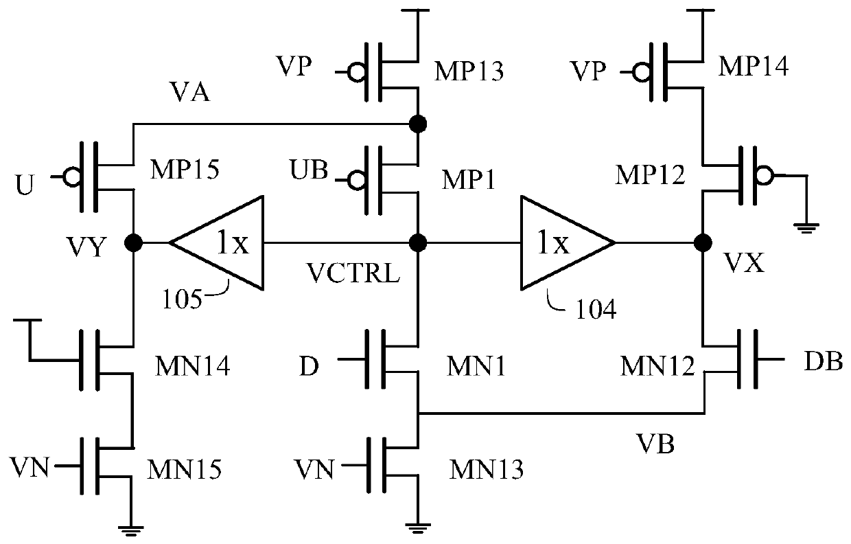
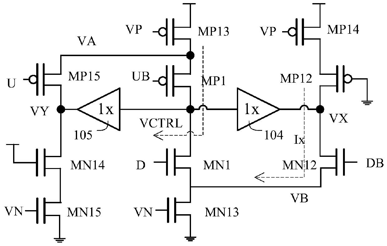
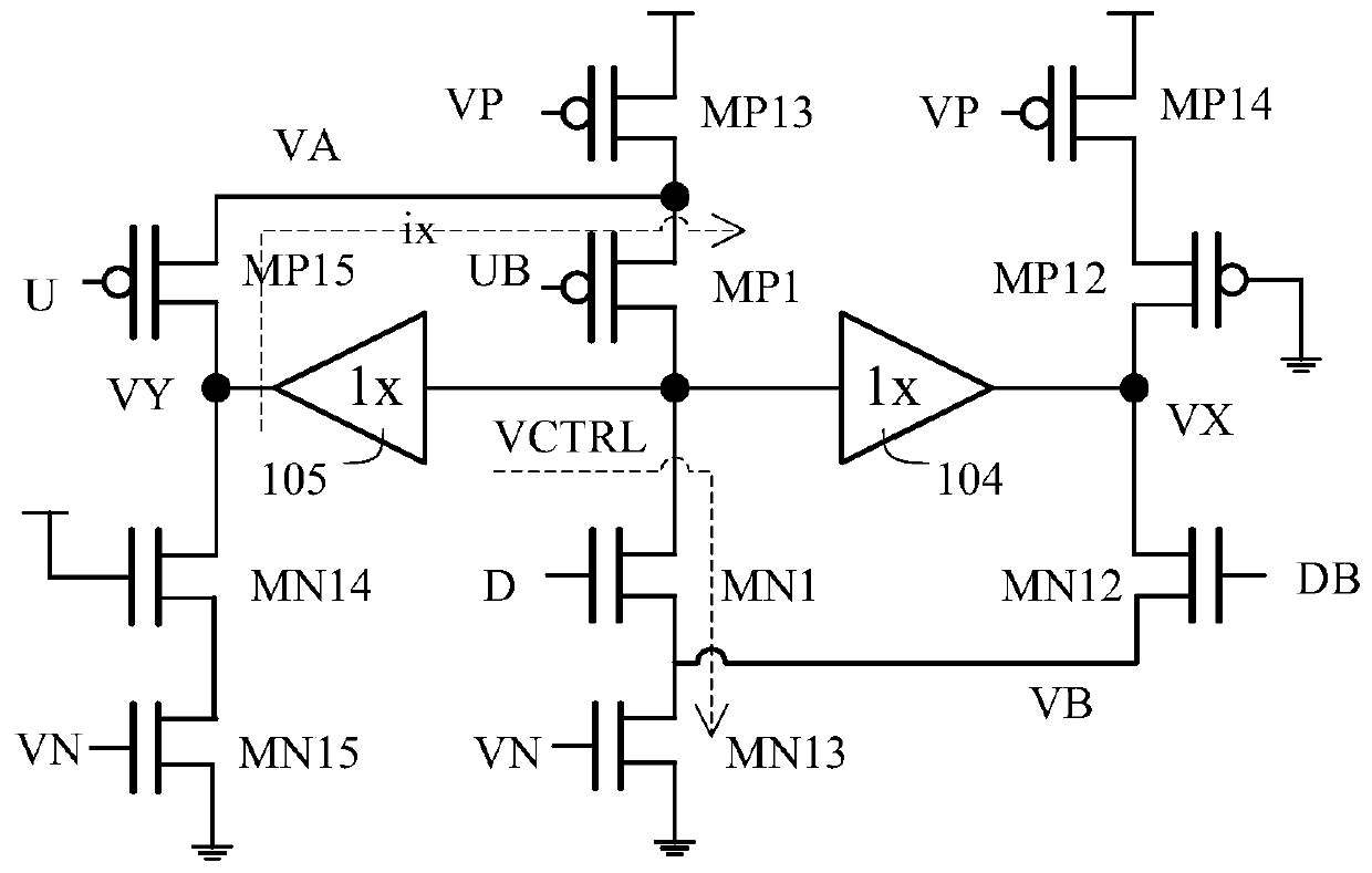
[0017] figure 1 is a schematic diagram of the charge pump circuit according to the first embodiment of the present invention. like figure 1 As shown, the charge pump circuit includes a charging and discharging main circuit, a first PMOS transistor MP1, and a first NMOS transistor MN1 are connected in series with each other on the charging and discharging main circuit, and the drains of MP1 and MN1 are connected at the node CTRL (marked by the voltage VCTRL ), the gate of MP1 is controlled by the inverse signal UB of the first control signal U, and the gate of MN1 is controlled by the second control signal D. In one example, the charge pump circuit may include a third PMOS transistor MP13, the drain of MP13 is connected to the source of MP1, the source is coupled to the power supply voltage, and the gate is controlled...


PUM


Abstract

An embodiment of the present invention provides a charge pump circuit. The circuit includes a first PMOS transistor and a first NMOS transistor connected in series on the charge and discharge main circuit, the gate of the first PMOS transistor is controlled by the inverse signal of the first control signal, and the gate of the first NMOS transistor is controlled by the second control signal Control; including the second PMOS transistor on the first branch, the gate is controlled by the first control signal; including the second NMOS transistor on the second branch, the gate is controlled by the inverse signal of the second control signal; wherein, in different Under the control of the first control signal and the second control signal, the first node where the drain of the first PMOS transistor is located, the second node where the drain of the second PMOS transistor is located, and the third node where the drain of the second NMOS transistor is located Nodes maintain the same or similar voltages. Embodiments of the present invention solve the problem of leakage current. At the same time, in different stages, since the voltages between corresponding nodes are equal or approximately the same, there is no need for voltage recovery.

Description

technical field [0001] This invention relates to electronic devices, and more particularly to charge pumps. Background technique [0002] A charge pump, also known as a switched capacitor voltage converter, is a type of DC-DC (converter) that uses so-called "flying" or "pumping" capacitors to store energy. They can step up or down the input voltage and can also be used to generate negative voltages. Its internal FET switch array controls the charging and discharging of the flying capacitor in a certain way, so that the input voltage is multiplied or reduced by a certain factor, so as to obtain the required output voltage. This special modulation process can guarantee up to 80% efficiency, and only external ceramic capacitors are needed. [0003] In current electronic devices, MOS transistors are usually used to implement charge pump circuits. However, since the MOS transistor has a certain degree of leakage current, the charge pump has a certain degree of leakage current,...

Claims


Application Information

Patent Timeline
Patent Type & Authority Patents(China)
IPC IPC(8): H02M3/07
CPCH02M3/07H02M3/078
Inventor 麦日锋
Owner CAPITAL MICROELECTRONICS
Why Eureka
Try Eureka