
Dual dielectric broadband infrared wave-absorbing metamaterial and design method thereof

A metamaterial and dual-media technology, applied in optics, instruments, optical components, etc., can solve problems such as complex design, poor applicability, and limited bandwidth, and achieve the effect of simple structure, convenient design, and easy fabrication

Active Publication Date: 2017-05-31
UNIV OF ELECTRONIC SCI & TECH OF CHINA
View PDF3 Cites 13 Cited by
  • Summary
  • Abstract
  • Description
  • Claims
  • Application Information

AI Technical Summary

Problems solved by technology

[0004] Therefore, the existing infrared artificial electromagnetic materials have defects such as complex design, complex process, limited bandwidth, and poor applicability.

Method used


Image

  • Dual dielectric broadband infrared wave-absorbing metamaterial and design method thereof
  • Dual dielectric broadband infrared wave-absorbing metamaterial and design method thereof
  • Dual dielectric broadband infrared wave-absorbing metamaterial and design method thereof

Examples


Embodiment 1

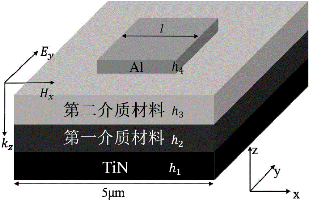
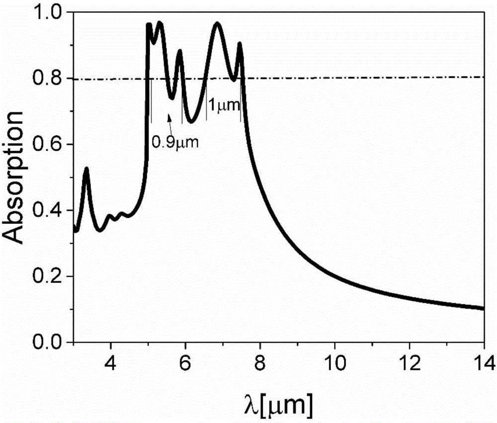
[0025] Dual-dielectric infrared absorbing metamaterials with a broadband absorption range of 5-8 μm, from bottom to top are TiN thin film, ZnSe thin film, MgF thin film and Al grating.

[0026] The thickness of the TiN film is 200nm, the thickness of the ZnSe film is 400nm, the thickness of the MgF film is 500nm, and the thickness of the Al grating is 60nm. The unit structure of the Al grating is composed of metal squares, the side length of the metal square is 1.7 μm, and the unit period is 5 μm. The simulation results obtained by the strict coupled wave method are as follows: figure 2 As shown, in the range of 5 μm-8 μm, the bandwidth of this embodiment at 80% absorption rate is 1.9 μm.

Embodiment 2

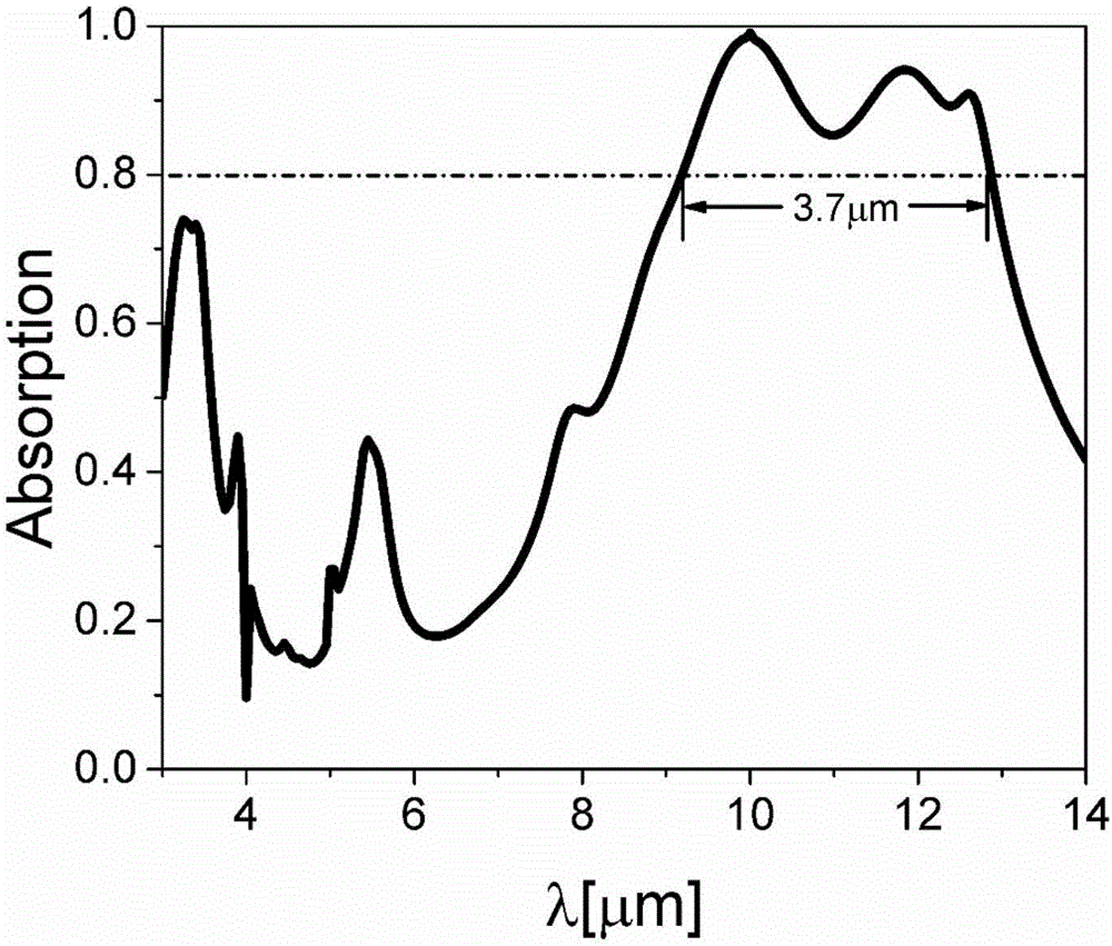
[0028] Dual-dielectric infrared absorbing metamaterials with a broadband absorption range of 8-14 μm, from bottom to top are TiN thin film, Ge thin film, ZnO thin film and Al grating.

[0029] The thickness of the TiN film is 200nm, the thickness of the Ge film is 600nm, the thickness of the ZnO film is 200nm, and the thickness of the Al grating is 130nm. The unit structure of the Al grating is composed of metal squares, the side length of the metal square is 2 μm, and the unit period is 5 μm. The simulation results obtained by the strict coupled wave method are as follows: image 3 As shown, in the range of 8 μm-14 μm, the bandwidth of this embodiment at 80% absorption rate is 3.7 μm.

[0030] In summary, the present invention is convenient in design, simple in structure and easy to manufacture. In the range of 5 μm-8 μm, the bandwidth of the present invention at 80% absorption rate reaches 1.9 μm; in the range of 8 μm-14 μm, the bandwidth of the present invention at 80% ab...


PUM

PropertyMeasurementUnit
Side lengthaaaaaaaaaa
Thicknessaaaaaaaaaa
Thicknessaaaaaaaaaa

Abstract

The invention belongs to the field of infrared manual electromagnetic metamaterials, in particular to a dual dielectric broadband infrared wave-absorbing metamaterial and a design method thereof. The metamaterial comprises a TiN membrane, a first dielectric material film, a second dielectric material film and a metal grating from bottom to top in sequence. In the dual dielectric broadband infrared wave-absorbing metamaterial, the high dielectric feature of the first dielectric material film is used for exciting a standing wave, a metal grating is used for exciting an air-metal surface plasma element, the metal grating and a TiN substrate are used for exciting magnetic resonance, and the second dielectric material film is used for reducing the excitation wavelength of the magnetic resonance, the standing wave, the surface plasma element and the magnetic resonance are coupled by adjusting the size of the grating, the material of a dielectric layer and the thickness of the dielectric layer, and a broadband wave-absorbing effect is achieved at different infrared wavebands. The dual dielectric broadband infrared wave-absorbing metamaterial is convenient in design, is simple in structure, and is easy to manufacture. The bandwidth at 80-percent absorbing rate is up to 1.9mum within the waveband range of 5mum to 8mum, and the bandwidth at 80-percent absorbing rate is up to 3.7mum within the waveband range of 8mum to 14mum.

Description

technical field [0001] The invention belongs to the field of infrared artificial electromagnetic metamaterials, and relates to a double-medium broadband infrared absorbing metamaterial and a design method thereof. Background technique [0002] With the rapid development of artificial electromagnetic metamaterials, compared with traditional electromagnetic materials, infrared artificial electromagnetic metamaterials have attracted more and more attention because of their negative refractive index, perfect absorption and selective absorption. Broadband infrared absorption has always been a research hotspot in infrared artificial electromagnetic metamaterials. On the one hand, according to the Plank law of thermodynamics, for an object with a surface temperature between zero and one thousand degrees, its main infrared radiation band is located at 2 μm-14 μm. On the other hand, due to the different degrees of absorption of electromagnetic waves in different bands by the atmosph...

Claims


Application Information

Patent Timeline
IPC IPC(8): G02B1/00G02B5/20G02B5/22
CPCG02B1/002G02B5/208G02B5/22
Inventor 周佩珩甄国帅杨林邓龙江
Owner UNIV OF ELECTRONIC SCI & TECH OF CHINA
Learn More