Wavelength-tunable FP optical fiber filter based on MEMS and preparation method thereof
A technology of optical fiber filter and optical fiber collimator, which is applied in the field of sensing, can solve problems such as the inability to find a balance, and achieve the effects of batch production, lower driving voltage, and low cost
- Summary
- Abstract
- Description
- Claims
- Application Information
AI Technical Summary
Problems solved by technology
Method used
Image
Examples
Embodiment 1
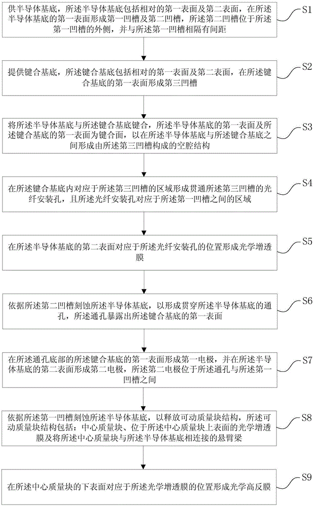
[0083] see figure 1 , the present invention provides a kind of preparation method based on MEMS wavelength tunable FP optical fiber filter, described preparation method based on MEMS wavelength tunable FP optical fiber filter comprises the following steps:
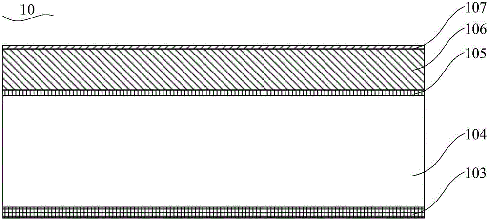
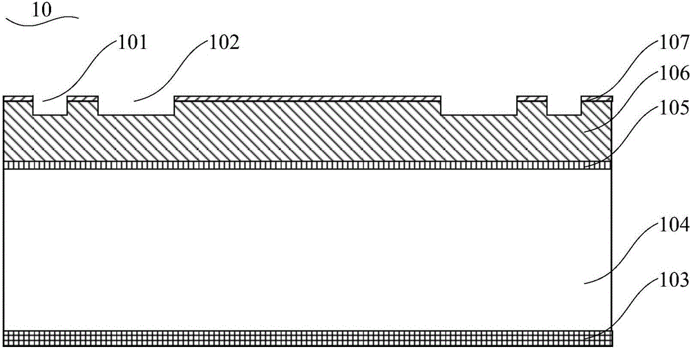
[0084] 1) A semiconductor substrate is provided, the semiconductor substrate includes opposite first surfaces and second surfaces, a first groove and a second groove are formed on the first surface of the semiconductor substrate, and the second groove is located on the the outer side of the first groove and is spaced apart from the first groove;
[0085] 2) Provide a bonding substrate, the bonding substrate includes opposite first surfaces and second surfaces, a third groove is formed on the first surface of the bonding substrate; the first groove is located on the third In the region corresponding to the groove, the second groove is located outside the third groove and is spaced from the edge of the third groove;
[008...
Embodiment 2
[0128] read on Figure 13 and Figure 14 , the present invention also provides a MEMS-based wavelength tunable FP optical fiber filter, the MEMS-based wavelength tunable FP optical fiber filter is prepared by the preparation method described in Embodiment 1, and the MEMS-based wavelength tunable FP Optical fiber filter comprises: semiconductor substrate 10, and described semiconductor substrate 10 comprises opposite first surface and second surface; The through hole (being the through hole 108 described in embodiment one that is formed with up and down penetrating in described semiconductor substrate 10) ); the semiconductor substrate 10 is a ring structure; the bonding substrate 11, the bonding substrate 11 includes opposite first surfaces and second surfaces, the first surface of the bonding substrate 11 is formed with grooves (i.e. implementing The third groove 111 described in Example 1), the optical fiber installation hole 112 that passes through the groove up and down i...
PUM
| Property | Measurement | Unit |
|---|---|---|
| Thickness | aaaaa | aaaaa |
| Thickness | aaaaa | aaaaa |
| Thickness | aaaaa | aaaaa |
Abstract
Description
Claims
Application Information
 - R&D Engineer
- R&D Manager
- IP Professional
- Industry Leading Data Capabilities
- Powerful AI technology
- Patent DNA Extraction
Browse by: Latest US Patents, China's latest patents, Technical Efficacy Thesaurus, Application Domain, Technology Topic, Popular Technical Reports.
© 2024 PatSnap. All rights reserved.Legal|Privacy policy|Modern Slavery Act Transparency Statement|Sitemap|About US| Contact US: help@patsnap.com


