Display panel and display device

A display panel and display device technology, applied in nonlinear optics, instruments, optics, etc., can solve the problems of affecting the brightness and contrast of the display device, low light injection efficiency, etc., to ensure the packaging effect, improve the light import efficiency, and avoid absorption. Effect

Active Publication Date: 2017-05-31
BOE TECH GRP CO LTD
View PDF3 Cites 5 Cited by
  • Summary
  • Abstract
  • Description
  • Claims
  • Application Information

AI Technical Summary

Problems solved by technology

[0003] For transparent display, in order to improve the transmittance, the light source is generally arranged on the side of the display panel, and in order to avoid the pollution of the light source to the liquid crystal, the light source is generally located outside the sealant, but the light source is located outside the sealant. Obviously, the frame sealant will reflect and absorb a large amount of incident light, resulting in low light injection efficiency and affecting the brightness and contrast of the display device

Method used


Image

  • Display panel and display device
  • Display panel and display device
  • Display panel and display device

Examples


Embodiment 1

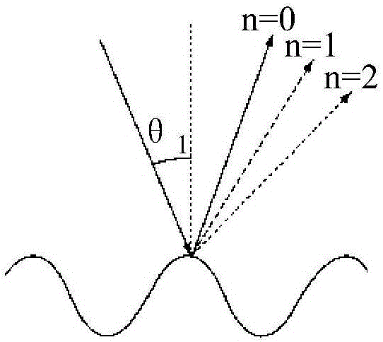
[0029] This embodiment provides a display panel, including a first substrate and a second substrate oppositely arranged, a liquid crystal cell located between the first substrate and the second substrate, and a liquid crystal cell for bonding the first substrate and the second substrate. A frame sealant, the surface of the first substrate facing the second substrate is provided with a light reflection structure, and the light reflection structure can reflect the light incident into the display panel from the second substrate side, so that The incident light is totally reflected multiple times in the display panel.

[0030] In this embodiment, the light source is arranged on the outside of one of the substrates of the display panel, and the light incident from the light source into the display panel is reflected by a light reflection structure, so that the incident light is totally reflected multiple times in the display panel, along the The direction parallel to the substrates...

Embodiment 2

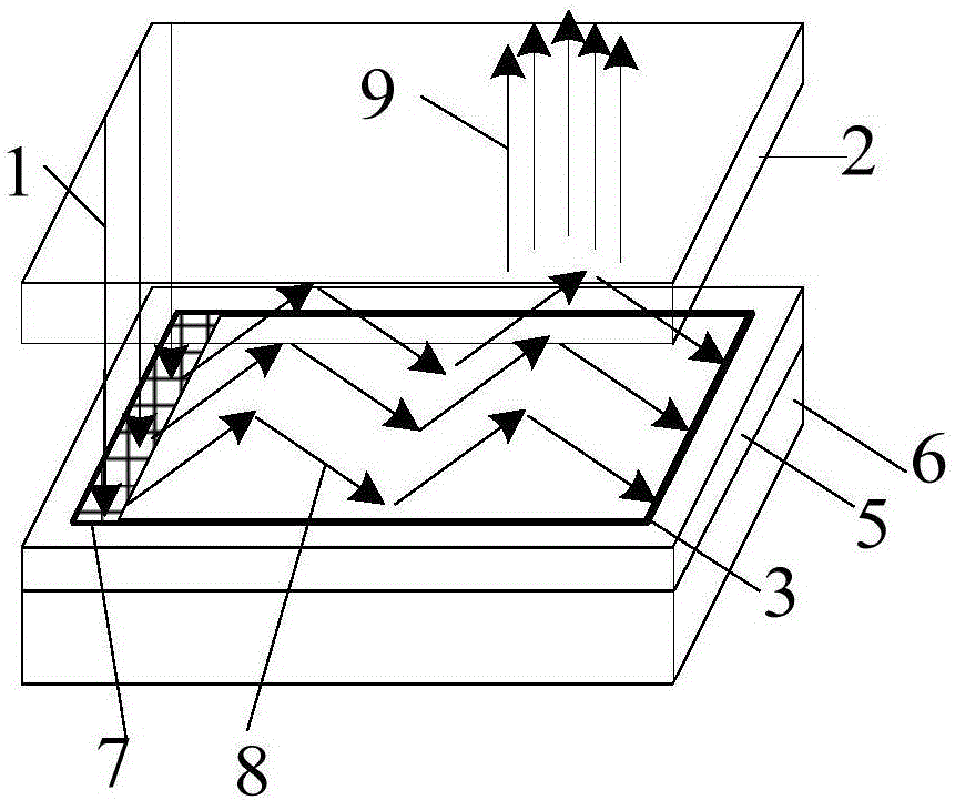
[0040] This embodiment provides a display device, which includes the above-mentioned display panel, and also includes a light source arranged on the surface of the second substrate facing away from the first substrate, and the light reflection structure faces the The light output side of the light source.

[0041] In this embodiment, the light source is arranged on the outside of one of the substrates of the display panel, and the light incident from the light source into the display panel is reflected by a light reflection structure, so that the incident light is totally reflected multiple times in the display panel, along the The direction parallel to the substrates propagates within the display panel. Because the light source of the present invention is arranged outside the display panel, it can ensure the encapsulation effect of the liquid crystal cell; in addition, because the light source is not arranged on the side of the display panel, it can avoid the absorption of in...

Embodiment 3

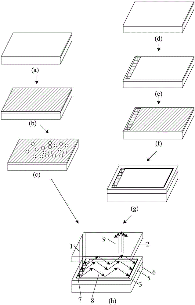
[0046] This embodiment provides a method for manufacturing a display panel, such as image 3 As shown, this embodiment specifically includes:

[0047] Step a: provide a second substrate 2, the second substrate 2 can be a quartz substrate or a glass substrate, the second substrate 2 is cleaned, and then an ITO layer is sputtered on the second substrate 2, and the thickness of the ITO layer can be 180- 220nm, pattern the ITO layer to form a common electrode;

[0048] Step b: performing PI film coating and orientation on the second substrate 2 formed with the common electrode;

[0049] Specifically, polyimide (PI) is coated on the side where the common electrode is formed on the second substrate 2, which can be put into a liquid crystal substrate spin coater for spin coating, and the rotation speed is set to 2500 rotations for 120s; The coated second substrate 2 is placed in a glass container, then placed in an oven, dried and preheated for 30 minutes at 80°C, and then baked fo...


PUM

PropertyMeasurementUnit
thicknessaaaaaaaaaa

Abstract

The invention provides a display panel and a display device and belongs to the technical field of display. The display panel comprises a first substrate, a second substrate, a liquid crystal box and a seal agent, wherein the first substrate and the second substrate are arranged oppositely, the liquid crystal box is positioned between the first substrate and the second substrate, and the seal agent is used for adhering the first substrate to the second substrate. Ray reflecting structures are arranged on the surface, facing the second substrate, of one side of the first substrate and are capable of reflecting rays incident into the display panel from the second substrate, so that incident rays are subjected to total reflection in the display panel for many times. The display panel is capable of improving brightness and contrast.

Description

technical field [0001] The present invention relates to the field of display technology, in particular to a display panel and a display device. Background technique [0002] In recent years, various display devices represented by liquid crystal displays have been rapidly developed and widely used due to their advantages such as low energy consumption, excellent display performance, and no radiation. In this kind of device manufacturing process based on the liquid crystal cell technology, a very important step is to use the sealing glue to make the upper and lower substrates tightly bonded, so as to cut off the contact between the liquid crystal molecules and the outside world, and prevent external air, water mist and other impurities from entering and polluting For liquid crystal, the sealant can also maintain the thickness of the box between the upper and lower substrates. [0003] For transparent display, in order to improve the transmittance, the light source is generall...

Claims


Application Information

Patent Timeline
Patent Type & Authority Applications(China)
IPC IPC(8): G02F1/1335
CPCG02F1/133553G02F1/133567
Inventor 雎长城王龙
Owner BOE TECH GRP CO LTD
Why Eureka
Try Eureka