
Photomask structure and COA-type array substrate

A technology of a photomask and a light-shielding part, which is applied in the field of liquid crystal display device manufacturing, can solve the problems such as the thickness and slope of the color filter layer 200 are not easy to control, gas leakage, and reduce the pixel aperture ratio, so as to avoid poor display, ease the slope, The effect of improving the quality of electrical connections

Active Publication Date: 2017-05-31
WUHAN CHINA STAR OPTOELECTRONICS TECH CO LTD
View PDF5 Cites 8 Cited by
  • Summary
  • Abstract
  • Description
  • Claims
  • Application Information

AI Technical Summary

Problems solved by technology

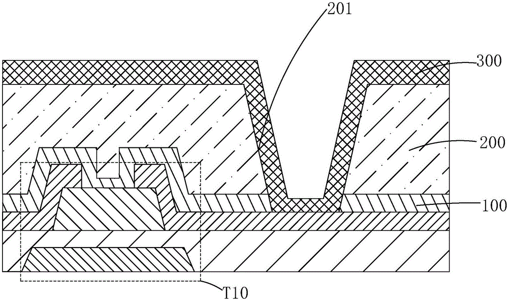
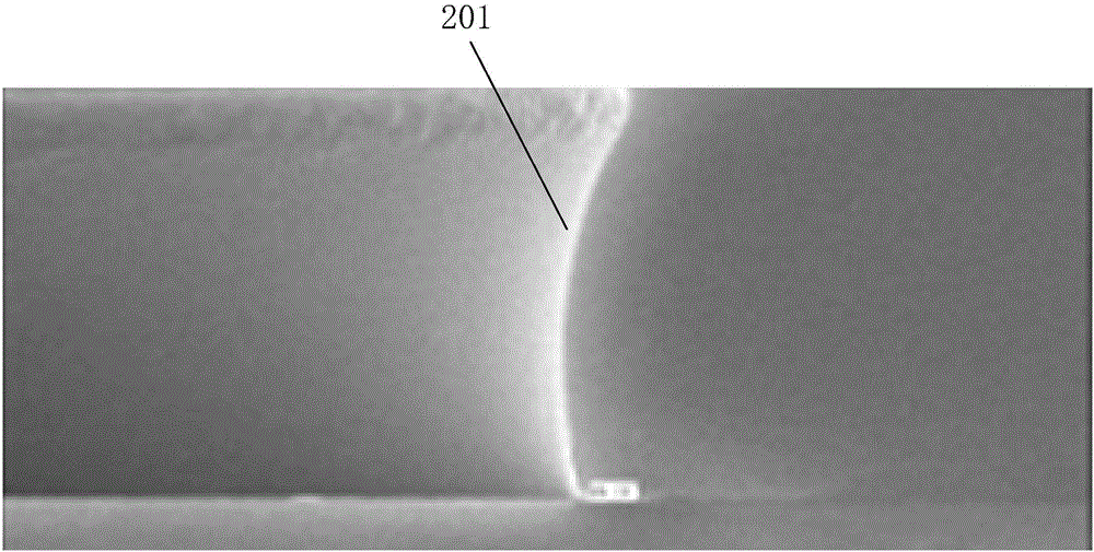
However, if image 3 As shown, using the above-mentioned existing photomask to make the via hole 201 in the color filter layer 200 will make the thickness and slope (Taper) of the color filter layer 200 at the via hole 201 difficult to control, and the slope is relatively steep, which is easy to cause The pixel electrode 300 in the via hole 201 breaks, resulting in poor electrical connection between the pixel electrode 300 and the metal signal line, resulting in poor display of the product
To ensure a good electrical connection, it is necessary to make a via hole 201 with a larger size, which will undoubtedly reduce the pixel aperture ratio, and if the via hole 201 is too large, the gas will easily leak out due to vibration after the box alignment process. And diffuse to the liquid crystal layer, resulting in bubbles (Bubble) and the formation of black clusters, affecting the display effect

Method used


Image

  • Photomask structure and COA-type array substrate
  • Photomask structure and COA-type array substrate
  • Photomask structure and COA-type array substrate

Examples


Embodiment Construction

[0031] In order to further illustrate the technical means adopted by the present invention and its effects, the following describes in detail in conjunction with preferred embodiments of the present invention and accompanying drawings.

[0032] Please also see Figure 4 to Figure 7 , the present invention provides a photomask structure for making color filter layer via holes in a COA-type array substrate, the photomask structure includes a central light-shielding part 1, surrounding the central light-shielding part 1 and connecting with the outer surface of the central light-shielding part 1 The peripheral light-shielding part 3 with the same contour shape, and the ring-shaped hollow slit 5 sandwiched between the peripheral light-shielding part 3 and the central light-shielding part 1 .

[0033] The photomask of the present invention is used together with negative photoresist, and the pattern jointly formed by the central light-shielding part 1 , the hollow slit 5 , and the pe...


PUM

PropertyMeasurementUnit
Widthaaaaaaaaaa
Widthaaaaaaaaaa

Abstract

The invention provides a photomask structure and a COA-type array substrate. The photomask structure comprises a center shading part (1), a peripheral shading part (3) and an annular hollowed-out slit (5), wherein the peripheral shading part (3) surrounds the center shading part (1) and is consistent with the center shading part (1) in outline shape; the annular hollowed-out slit (5) is clamped between the peripheral shading part (3) and the center shading part (1); and exposure light is diffracted through the hollowed-out slit (5), is bent and scattered in opposite directions, generates a gradual change of energy intensity, and is matched with a negative photoresist, so that the slope of the finally prepared color film via hole can be alleviated, the electric connection quality between a pixel electrode and a signal line of a metal material is improved and poor display is avoided.

Description

technical field [0001] The invention relates to the field of liquid crystal display device manufacturing process, in particular to a photomask structure and a COA type array substrate. Background technique [0002] With the continuous development of display technology, thin film transistor liquid crystal display (Thin Film Transistor Liquid Crystal Display, TFT-LCD) has been widely used in Various consumer electronic products such as mobile phones, televisions, personal digital assistants, digital cameras, notebook computers, and desktop computers have become the mainstream of flat panel display devices. [0003] Most of the liquid crystal displays currently on the market are backlight liquid crystal displays, which include a liquid crystal display panel and a backlight module. A traditional liquid crystal display panel is composed of a color filter substrate (Color Filter, CF), a thin film transistor array substrate (Thin Film Transistor Array Substrate, TFT Array Substrat...

Claims


Application Information

Patent Timeline
IPC IPC(8): G03F7/20H01L27/12
CPCG03F7/70283H01L27/1244G03F1/36G03F1/38G03F7/0007H01L27/124
Inventor 孙涛
Owner WUHAN CHINA STAR OPTOELECTRONICS TECH CO LTD
Learn More