Jitter tolerance simulation verification method of clock data recovery circuit

A clock data recovery and jitter tolerance technology, which is applied in electrical digital data processing, CAD circuit design, special data processing applications, etc. The effect of reducing chip risk, implementing simplicity, and being easy to implement in engineering

Inactive Publication Date: 2017-05-31
UNIV OF ELECTRONICS SCI & TECH OF CHINA +1
View PDF2 Cites 5 Cited by
  • Summary
  • Abstract
  • Description
  • Claims
  • Application Information

AI Technical Summary

Problems solved by technology

You can refer to the idea of ​​testing when implementing simulation verification, but because superimposed jitter can only delay data backwards on the time axis during simulation verification, and cannot delay the superimposition in the opposite direction of the time axis, it is difficult to achieve the ideal jitter superposition effect

Method used


Image

  • Jitter tolerance simulation verification method of clock data recovery circuit
  • Jitter tolerance simulation verification method of clock data recovery circuit
  • Jitter tolerance simulation verification method of clock data recovery circuit

Examples


Embodiment Construction

[0027] In order to make the method and advantages of the present invention clearer and easier to understand, the design scheme of the jitter tolerance simulation verification method provided by the present invention will be described in detail below, but this does not constitute a limitation to the present invention.

[0028] The present invention is a jitter tolerance simulation verification method of a clock data recovery circuit, and its specific implementation steps include:

[0029] Phase 1: Verification module design for jitter tolerance.

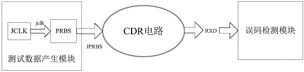
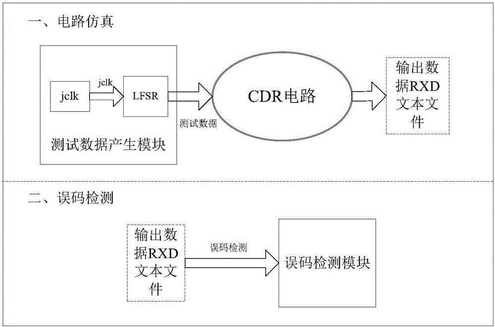
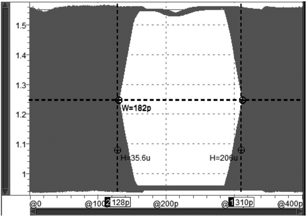
[0030] Step1: Design the verification module of jitter tolerance. The verification module of jitter tolerance includes two parts: test data generation module and error detection module. The test data generation module is used to generate a low-voltage serial differential signal containing jitter information, including a jitter modulation clock JCLK and a pseudo-random code generation module PRBS. The jitter modulation clock is realiz...


PUM


Abstract

The invention discloses a jitter tolerance simulation verification method of a clock data recovery circuit. The jitter tolerance simulation verification method is implemented through the following three modules: a test data generating module, a clock data recovery (CDR) circuit and an error code detection module, wherein the test data generating module generates a pseudo random sequence superposed with jitter information as an input of the CDR circuit, consists of a jitter modulating clock and a pseudo random code generating module, and is implemented via VerilogA language design; the error code detection module performs an error code detection on an output data file of CDR simulation, and is implemented through Python scripts. The jitter tolerance simulation verification method comprises the following two steps: first, simulating the test data generating module and the CDR circuit to obtain the output data file of the CDR; then, performing the error code detection on the output data file by using the error code detection module. By the jitter tolerance simulation verification method, the jitter resistance of the CDR is evaluated in a design stage, so that tape-out risks are effectively reduced; in addition, the jitter tolerance simulation verification method is easy to implement and short in verification time and has relatively strong practicability.

Description

technical field [0001] The invention discloses a method for simulating and verifying the jitter tolerance of a clock data recovery circuit, which can evaluate the anti-jitter performance of the receiving end in the design stage. Specifically, by adding jitter to the clock of the pseudo-random code generation module, the pseudo-random code with jitter is obtained as the serial input data of the CDR, and then the circuit simulation is performed to obtain the output data file of the CDR, and then the output data file of the CDR is processed. Error detection processing. Background technique [0002] With the rapid development of digital communication technology and the continuous improvement of data processing capabilities, the amount of information exchanged between chips, boards and systems has become larger and larger, which has resulted in I / O transmission rates becoming the bottleneck that limits system performance. Due to the impact of clock skew, crosstalk, coupling and ...

Claims


Application Information

Patent Timeline
Patent Type & Authority Applications(China)
IPC IPC(8): G06F17/50
CPCG06F30/33G06F30/396
Inventor 王忆文黄金凤刘云龙李大超
Owner UNIV OF ELECTRONICS SCI & TECH OF CHINA
Why Eureka
Try Eureka