Diamond heat sink GaN-based different-side electrode LED manufacturing method

A production method and diamond technology, applied in the direction of circuits, electrical components, semiconductor devices, etc., can solve the problems of complex process, limited thermal conductivity, affecting LED life and lighting performance, etc., to achieve simple process, avoid the impact of LED performance, The effect of heat dissipation is obvious

Active Publication Date: 2017-05-31
SHAANXI UNIV OF SCI & TECH
View PDF7 Cites 9 Cited by
  • Summary
  • Abstract
  • Description
  • Claims
  • Application Information

AI Technical Summary

Problems solved by technology

However, as the lighting power continues to increase, the heat generated by the LED will rise sharply. If the heat is not dissipated in time, the high temperature inside the LED due to heat will seriously affect the life and lighting performance of the LED. Therefore, heat dissipation has become an LED lighting technology. A key issue in the field that needs to be solved urgently
[0005] The traditional solution to LE

Method used


Image

  • Diamond heat sink GaN-based different-side electrode LED manufacturing method
  • Diamond heat sink GaN-based different-side electrode LED manufacturing method
  • Diamond heat sink GaN-based different-side electrode LED manufacturing method

Examples


Embodiment Construction

[0060] A method for manufacturing a diamond heat sink GaN-based different-side electrode LED, comprising the following steps:

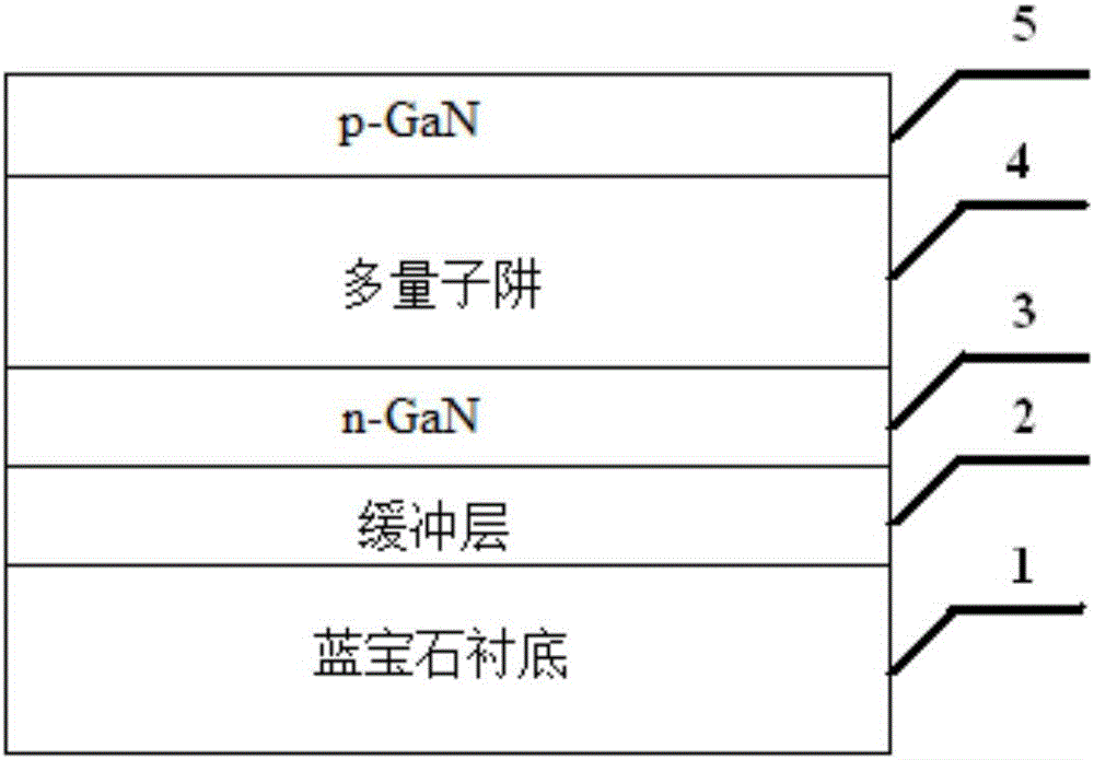
[0061] S1: MOCVD growth of GaN-based LED epitaxial material on sapphire substrate 1;

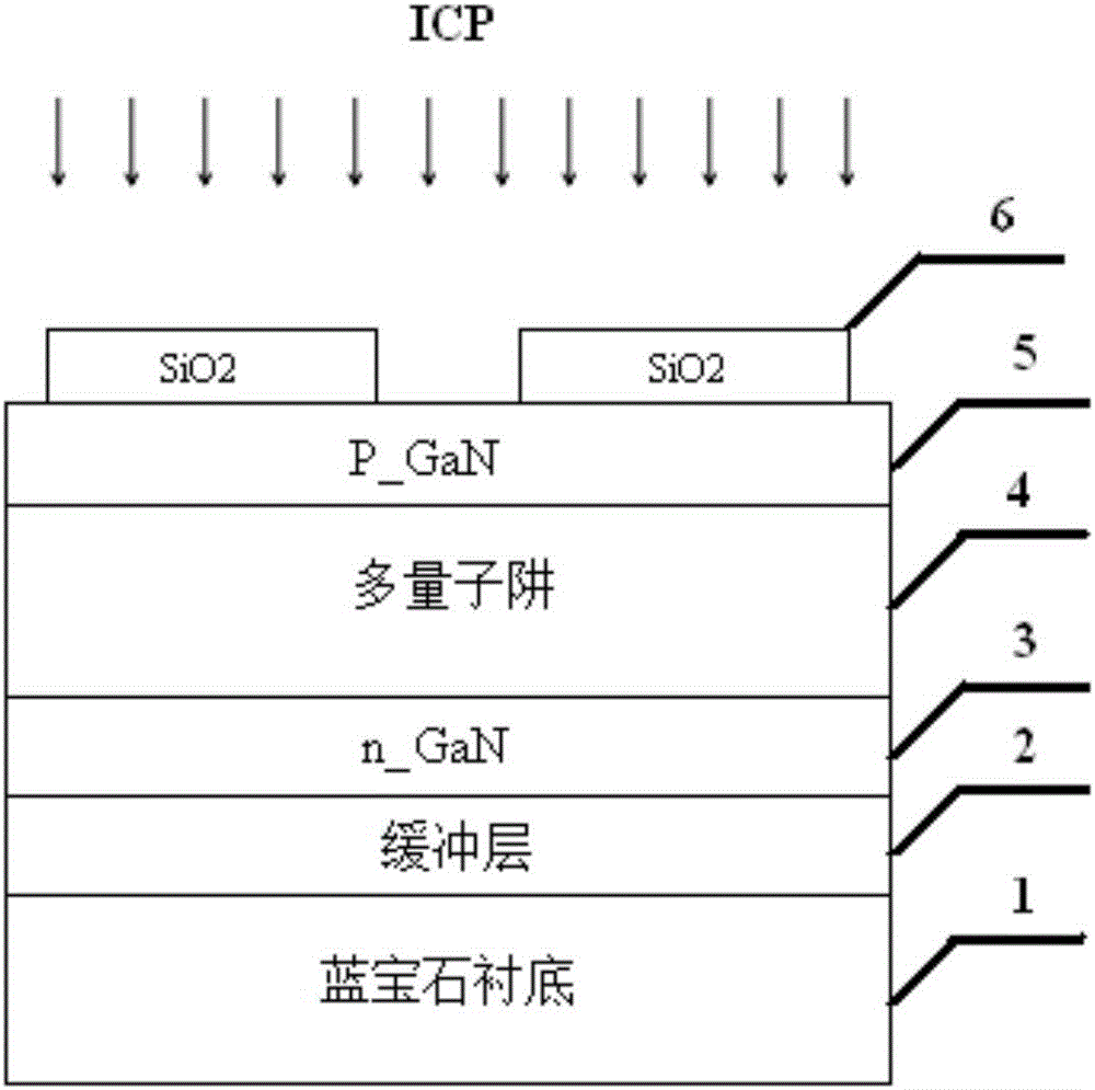
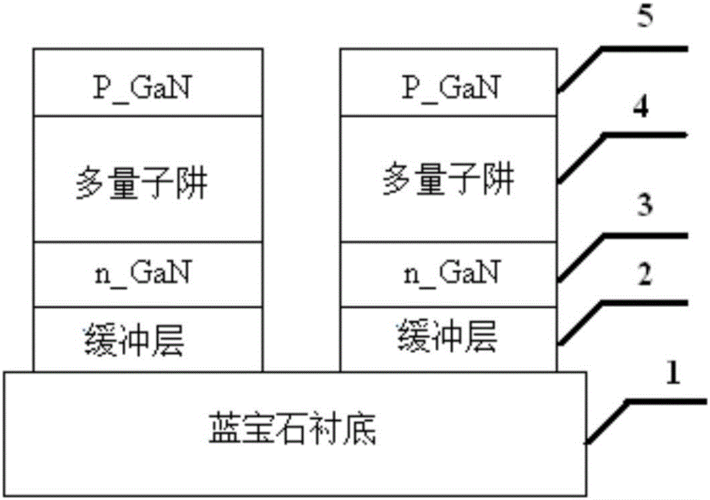
[0062] see figure 1 As shown, the sapphire substrate GaN-based LED epitaxial material is specifically, the sapphire substrate (0001) is polished on one side, the thickness is 500 μm, the thickness of the intrinsic GaN buffer layer 2 is 50 nm, and the thickness of the n-GaN layer 3 is 2 μm. The GaN / InGaN multiple quantum well 4, the p-GaN layer 5 has a thickness of 0.2 μm, and after the GaN-based LED epitaxial material is epitaxially grown on the sapphire substrate, the isolation groove is etched, including the following steps:

[0063] S11: cleaning the sapphire substrate, ultrasonication with acetone and deionized water for 2-3 minutes each.

[0064] S12: Put the sapphire substrate in H at 900-1000°C 2 Baking is carried out under the atmosphere to remove surface...


PUM

PropertyMeasurementUnit
Thicknessaaaaaaaaaa

Abstract

The present invention discloses a diamond heat sink GaN-based different-side electrode LED manufacturing method. The method comprises: performing MOCVD growth of GaN-based LED epitaxial materials on a sapphire substrate; performing ICP etching of the GaN-based LED epitaxial materials of the sapphire substrate, and performing device isolation; performing magnetron sputtering of p-type contact metal, reflective metal and bonding metal on the surfaces of the GaN-based LED epitaxial materials on the sapphire substrate; performing magnetron sputtering of the bonding metal on the surface of a diamond heat sink substrate; performing metal bonding of the GaN-based LED epitaxial materials of the sapphire substrate and the diamond heat sink substrate; performing stripping of the sapphire substrate through adoption of the laser stripping technology; and finally performing magnetron sputtering of n-type contact metal. The diamond heat sink GaN-based different-side electrode LED manufacturing method employs diamond with high heat conductivity to take as a heat sink, LED anodic metal is in metal bonding contact with the diamond, and the heat radiation advantage is obvious; the LED anodic metal is in metal bonding with the diamond in a low temperature to effectively avoid the influence of traditional high-temperature bonding on the LED performance; and the technology is simple in the sapphire substrate leaser stripping process.

Description

[0001] 【Technical field】 [0002] The invention belongs to the technical field of LED heat dissipation, and in particular relates to a method for manufacturing a diamond heat sink GaN-based different-side electrode LED. [0003] 【Background technique】 [0004] As the fourth-generation lighting source, GaN-based LED has the advantages of high efficiency, long service life, energy saving, and environmental protection, and has become a strategic emerging industry that focuses on development at home and abroad. However, as the lighting power continues to increase, the heat generated by the LED will rise sharply. If the heat is not dissipated in time, the high temperature inside the LED due to heat will seriously affect the life and lighting performance of the LED. Therefore, heat dissipation has become an LED lighting technology. It is a key issue that needs to be solved urgently. [0005] The traditional solution to LED heat dissipation is to use flip-chip welding technology to a...

Claims


Application Information

Patent Timeline
IPC IPC(8): H01L33/64H01L33/00
CPCH01L33/0066H01L33/0075H01L33/641H01L2933/0075
Inventor 王进军
Owner SHAANXI UNIV OF SCI & TECH
Why Eureka
Try Eureka