Film-expanding grain-eliminating method of wafer and wafer production method

A technology of wafers and grains, which is applied in the manufacture of electrical components, electrical solid devices, semiconductor/solid devices, etc., can solve problems such as low packaging efficiency, chipping of adjacent grains, and affecting the normal progress of the process, so as to improve The effect of packaging efficiency

Active Publication Date: 2017-06-09
JILIN MAGIC SEMICON
View PDF6 Cites 9 Cited by
  • Summary
  • Abstract
  • Description
  • Claims
  • Application Information

AI Technical Summary

Problems solved by technology

[0003] When the traditional die is packaged, it is necessary to sort the die first, and then remove the unqualified die before packaging, resulting in low packaging efficiency
In order to improve the packaging efficiency, some wafer manufacturers are now cutting the wafer into grains, and then rejecting the un...

Method used


Image

  • Film-expanding grain-eliminating method of wafer and wafer production method
  • Film-expanding grain-eliminating method of wafer and wafer production method

Examples


Embodiment 1

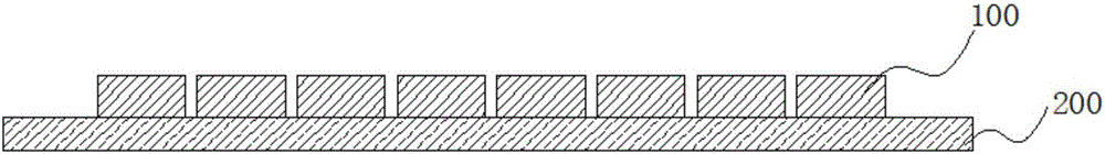
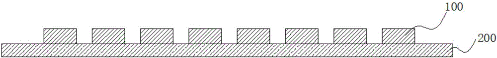
[0065] figure 1 A schematic diagram of the cross-sectional structure of the wafer before film expansion provided in Embodiment 1 of the present invention; figure 2 for figure 1 The schematic diagram of the cross-sectional structure of the wafer after film expansion is shown; figure 1 with figure 2 As shown, the embodiment of the present invention provides a wafer film expansion and particle extraction process, including the following steps:

[0066] (a) providing a wafer, the wafer is cut into a plurality of crystal grains 100, the multiple crystal grains 100 are adhered to the base film 200, the distance between the crystal grains 100 is 200 μm, and the base film 200 is fixed on the fixing ring, And the crystal grain 100 has passed the electrical performance test, and the unqualified grain is marked as black;

[0067] (b) Heat the stage of the film expander to 50°C, put the bottom film 200 with the crystal grains 100 attached on the stage of the film expander, fix the b...

Embodiment 2

[0074] The embodiment of the present invention provides a wafer production method. The unqualified crystal grains are removed by adopting the film expansion method provided by the embodiment of the present invention, so that there is no need to separate the grains during the subsequent packaging process. It only needs to be packaged directly, which effectively reduces the operation steps of the packaging process and improves the packaging efficiency.


PUM

PropertyMeasurementUnit
Thicknessaaaaaaaaaa

Abstract

The invention provides a film-expanding grain-eliminating method of a wafer and a wafer production method, wherein the film-expanding grain-eliminating method and the wafer production method relate to the technical field of semiconductor wafer processing. The film-expanding grain-eliminating method comprises the following steps of (a), supplying a wafer and cutting the wafer into a plurality of crystal grains which adhere a bottom film; (b), performing expansion on the bottom film on which the plurality of crystal grains are adhered, and eliminating the unqualified grain particles; and (c), baking the bottom film for restoring the bottom film to a state before film expansion. The film-expanding grain-eliminating method settles technical problems of edge breaking and scratch of adjacent crystal grains, severe crystal grain quality reduction and incapability of normally performing subsequent processes caused by mutual collision between the unqualified crystal grains and the adjacent crystal grains in an unqualified crystal grain eliminating process after the wafer is cut into crystal grains by a wafer manufacturer. Distance increase between the crystal grains is realized through film expansion so that the unqualified crystal grains do not collide with adjacent crystal grains in the eliminating process, thereby realizing technical effects of ensuring high crystal grain quality and facilitating subsequent normal execution of a subsequent packaging process.

Description

technical field [0001] The invention relates to the technical field of semiconductor wafer processing, in particular to a wafer film expanding and grain-taking method and a wafer production method. Background technique [0002] In recent years, with the rapid development of the optoelectronic industry, the demand for highly integrated and high-performance semiconductor wafers has also increased. In order to greatly save costs and improve manufacturing efficiency, integrated circuits are often deposited on wafers in mass production. The chip or circuit element structure is then divided into individual crystal grains, and finally packaged and soldered. Therefore, the packaging efficiency of the crystal grains has an important impact on improving the production efficiency of the wafer. [0003] When traditional dies are packaged, the dies need to be sorted first, and the unqualified dies can be removed before packaging, resulting in low packaging efficiency. In order to improv...

Claims


Application Information

Patent Timeline
IPC IPC(8): H01L21/683
CPCH01L21/6835H01L21/6836H01L2221/68336
Inventor 田振兴王斌张树宝孔玲娜
Owner JILIN MAGIC SEMICON
Why Eureka
Try Eureka