A kind of transparent electrode and preparation method thereof
A technology of transparent electrodes and transparent substrates, which is applied in the manufacture of circuits, electrical components, and final products. It can solve problems such as high light transmittance, achieve excellent electrical conductivity, expand the scope of optoelectronic applications, improve mechanical strength, and withstand distortion. effect of ability
- Summary
- Abstract
- Description
- Claims
- Application Information
AI Technical Summary
Problems solved by technology
Method used
Image

Examples
Embodiment 1
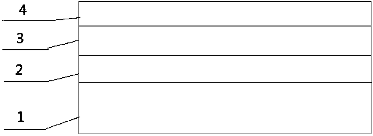
[0051] refer to figure 1 As shown, this embodiment provides a transparent electrode based on a broadband optically transparent continuous metal film layer and its preparation method, which can have the inherent perfect electrical conductivity characteristics of the metal film layer and also have excellent optical transparency characteristics.
[0052] The transparent electrode includes a transparent substrate 1 , a first high dielectric film layer 2 , a metal film layer 3 , and a second high dielectric film layer 4 from bottom to top.
[0053] The metal film layer is a continuous metal film layer; the continuous metal film layer means that the film layer itself has no voids / holes or cracks. Generally, if the metal film layer is too thin, it will be just a cluster of particles rather than a complete film layer that communicates with each other.
[0054] The dielectric constant of the high dielectric film layer is greater than or equal to 6.25.
[0055] High-dielectric materia...
Embodiment 2
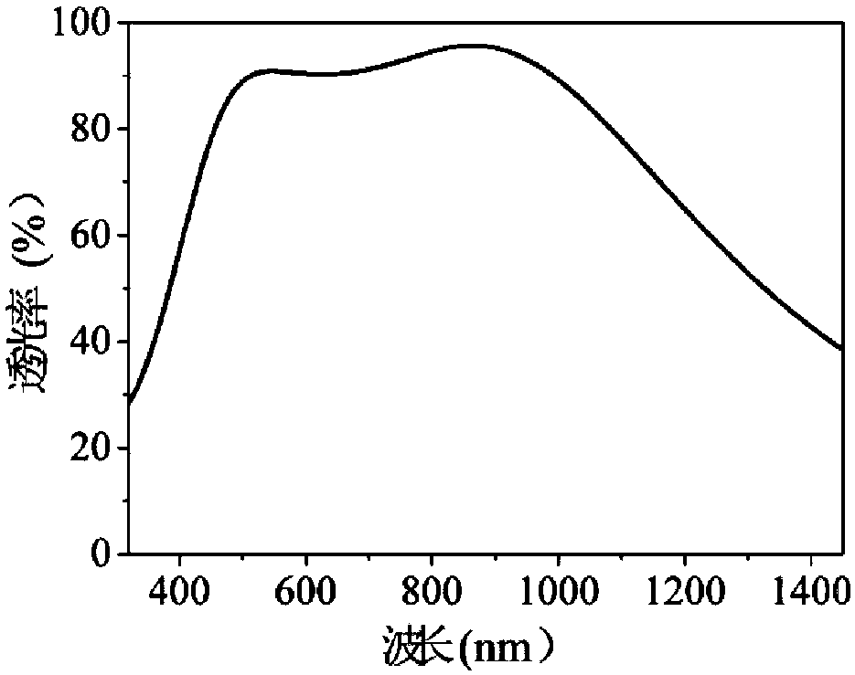
[0062] This embodiment provides a transparent electrode, including figure 1 The transparent substrate 1 , the first high dielectric film layer 2 , the metal film layer 3 , and the second high dielectric film layer 4 are arranged sequentially from bottom to top.
[0063] Wherein, the metal material of the metal film layer 3 is gold, the material of the high dielectric film layer is titanium dioxide, the thickness of the metal film layer 3, the thickness of the first high dielectric film layer 2 and the second high dielectric film layer 4 are respectively 15nm, 40nm, 40nm. The material of the transparent substrate 1 is polydimethylsiloxane (PDMS), a flexible substrate material, with a thickness of 5 microns.
[0064] The preparation method of the transparent electrode of this embodiment is the same as that of Embodiment 1, and will not be repeated here.
[0065] refer to figure 2 As shown, this embodiment is based on the light transmittance diagram of the transparent electro...
Embodiment 3
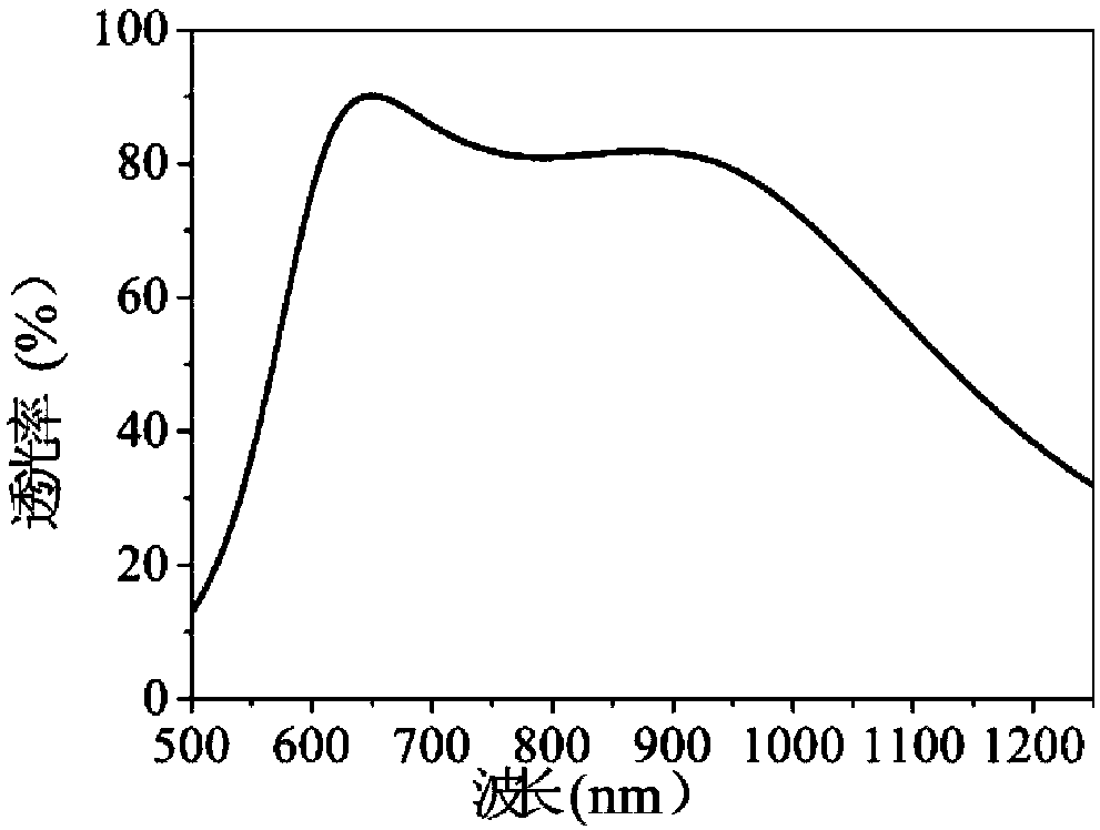
[0068] This embodiment provides a transparent electrode, including figure 1 The transparent substrate 1 , the first high dielectric film layer 2 , the metal film layer 3 , and the second high dielectric film layer 4 are arranged sequentially from bottom to top.
[0069] Wherein, the metal material of the metal film layer 3 is silver, the material of the high dielectric film layer is titanium dioxide, the thickness of the metal film layer 3, the thickness of the first high dielectric film layer 2 and the second high dielectric film layer 4 are respectively 15nm, 40nm, 40nm. The material of the transparent substrate 1 is polydimethylsiloxane (PDMS), a flexible substrate material, with a thickness of 5 microns.
[0070] The preparation method of the transparent electrode of this embodiment is the same as that of Embodiment 1, and will not be repeated here.
[0071] refer to image 3 As shown, this embodiment is based on the light transmittance diagram of the transparent electr...
PUM
| Property | Measurement | Unit |
|---|---|---|
| thickness | aaaaa | aaaaa |
| thickness | aaaaa | aaaaa |
| thickness | aaaaa | aaaaa |
Abstract
Description
Claims
Application Information
 - R&D
- Intellectual Property
- Life Sciences
- Materials
- Tech Scout
- Unparalleled Data Quality
- Higher Quality Content
- 60% Fewer Hallucinations
Browse by: Latest US Patents, China's latest patents, Technical Efficacy Thesaurus, Application Domain, Technology Topic, Popular Technical Reports.
© 2025 PatSnap. All rights reserved.Legal|Privacy policy|Modern Slavery Act Transparency Statement|Sitemap|About US| Contact US: help@patsnap.com