Bare chip structure applied to testing and manufacturing method thereof

A manufacturing method and bare chip technology, which is applied in semiconductor/solid-state device manufacturing, semiconductor/solid-state device components, semiconductor devices, etc., can solve the problem of high PCB processing accuracy and technical level requirements of bonding operators, and fixture development cycle It cannot meet the timeliness requirements of chip testing and the difficulty of effective connection, etc., and achieve the effect of good engineering application implementability, guaranteed reuse, and avoiding complicated steps and costs

Active Publication Date: 2017-06-16
上海鹏武电子科技有限公司
View PDF4 Cites 8 Cited by
  • Summary
  • Abstract
  • Description
  • Claims
  • Application Information

AI Technical Summary

Problems solved by technology

[0003] Wafer-level testing can test bare chips through wafer probes and special test benches, but it can only complete relatively simple test tasks, and has more limitations in testing the actual functions of chips; some foreign companies have launched KGD ( Known Good Die) bare chip products, using special fixtures to test bare chips, the special customization of fixtures and development cycle still cannot meet the timeliness requirements of chip testing; at present, it is more common to fix the bare chip on the PCB board, Use a bonding machine to connect the chip pins and PCB board pads, and then use special glue to cover and protect the entire structure, so that the chip can be fully functionally tested in the laboratory environment
However, once the glue is cured, it is difficult to remove from the bare core, and the maintainability is not good, and the process of covering the bare chip with the glue may cause contact and connection between the bonding wires, resulting in poor reliability.
With the increasing complexity of chips and hundreds of functional pins, it is necessary to process the same number of bonding pads on the PCB as bonding points. Due to the length requirements of bonding wires, metal bonding soldering The disk area and spacing are limited, and it is very easy to cause contact connection between the bonding wires during bonding. The requirements for the processing accuracy of the PCB board and the technical level of the bonding operator are high, and multi-pin bare chips can be realized under ordinary laboratory conditions. It is more difficult to effectively connect with the PCB board; and the larger the area of ​​the bare chip, the more conductive glue is required for bonding on the PCB board. When the bare chip is pressed on the PCB board, the conductive glue will be on the bare chip. The overflow on the side is very easy to adhere to the metal pad of the bare chip, forming a short circuit between the metal pads, causing the bare chip to be scrapped

Method used


Image

  • Bare chip structure applied to testing and manufacturing method thereof
  • Bare chip structure applied to testing and manufacturing method thereof
  • Bare chip structure applied to testing and manufacturing method thereof

Examples


Embodiment 1

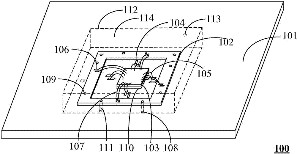
[0052] See figure 1 , figure 1 A schematic structural diagram of a bare chip structure applied to testing provided by an embodiment of the present invention, wherein the structure 100 includes: a main PCB board 101, a secondary PCB board 102, a bare chip 103, a first pad 104, a first key Aligning wire 105 , second pad 106 , second bonding wire 107 , pad 110 , metal pin header 111 , protective cover 112 and electrical insulating oil 114 .

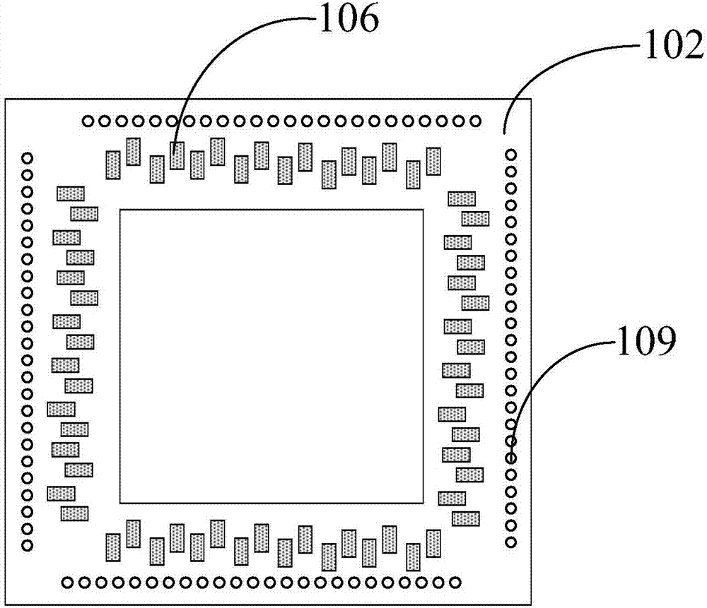
[0053] Wherein, the pad 110 is bonded to the main PCB 101 and the bare chip 103 is bonded to the pad 110; the first solder pad 104 surrounds the bare chip 103 and is arranged On the main PCB 101 and connected to the metal PAD of the bare chip 103 through the first bonding wire 105; the secondary PCB 102 is located on the periphery of the first pad 104 and bonded to On the main PCB board 101 and realize electrical connection with the main PCB board 101 through the metal pin 111; the second pad 106 is arranged on the secondary PCB board 102 ...

Embodiment 2

[0073] See Figure 7 , Figure 7 It is a schematic flowchart of a method for manufacturing a bare chip structure applied to testing provided by an embodiment of the present invention. Wherein, the manufacturing method includes:

[0074] Making the main PCB board 101, and making the first pad 104 on the surface of the main PCB board 101;

[0075] Adhesive pads 110 at specified positions on the surface of the main PCB 101 and bond bare chips 103 on the surface of the pads 110;

[0076] Bonding both ends of the first bonding wire 105 to the metal PAD of the bare chip 103 and the first pad 104 using a bonding process;

[0077] Make the secondary PCB board 102, and make the second pad 106 on the surface of the secondary PCB board 102;

[0078] Bonding the secondary PCB board 102 on the main PCB board 101;

[0079] The two ends of the second bonding wire 107 are bonded to the metal PAD of the bare chip 103 and the second pad 106 using a bonding process, and the metal pin 111 is...

Embodiment 3

[0089] See Figure 8 , Figure 8 It is a schematic flowchart of another method for manufacturing a bare chip structure applied to testing provided by an embodiment of the present invention. Wherein, the manufacturing method includes:

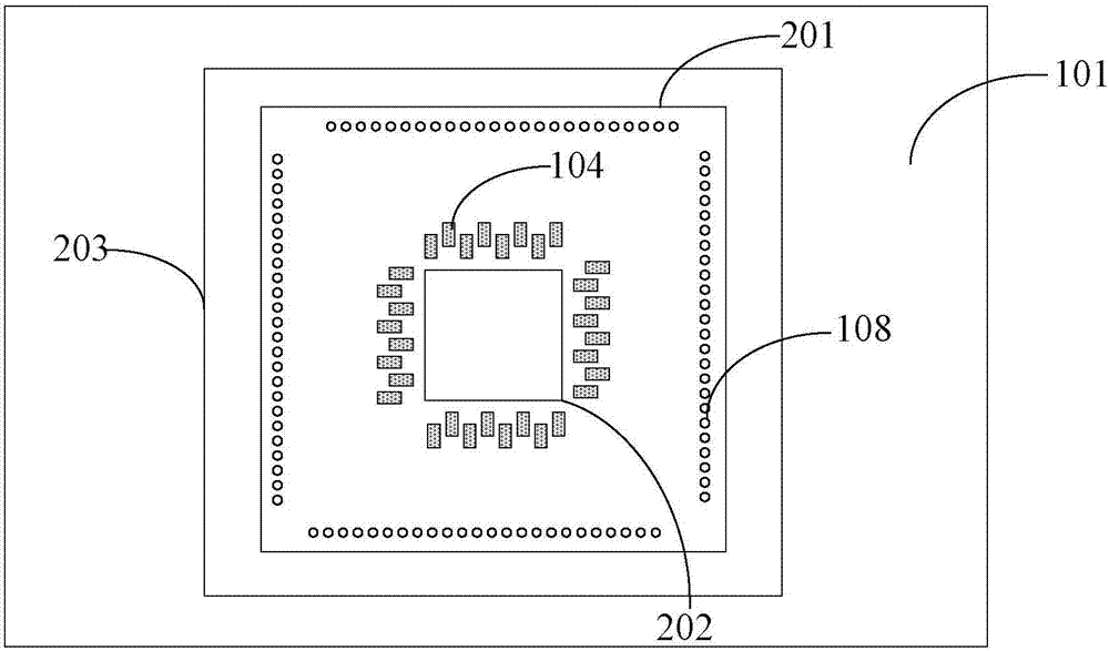
[0090] Select the main PCB board 101, and make the first boundary line 201 of the bonding secondary PCB board 102, the second boundary line 202 of the bonding gasket 110 and the third boundary line of the bonding protective cover 112 on the surface of the main PCB board 101 203; and on the surface of the main PCB 101 along the periphery of the second boundary line 202, make the first pads 104 in a staggered arrangement;

[0091] The gasket 110 is bonded on the surface of the main PCB 101 along the second boundary line 202 and the bare chip 103 is bonded on the surface of the gasket 110, and the first bonding wire 105 is used to connect all The metal PAD of the bare chip 103 and the first pad 104;

[0092] Select the secondary PCB board 102 t...


PUM


Abstract

The invention discloses a bare chip structure applied to testing and a manufacturing method thereof. The bare chip structure 100 comprises a main PCB (Printed Circuit Board) 101, a subsidiary PCB 102, a bare chip 103, bonding pads 104 / 106, bonding wires 105 / 107, a gasket 110, metal header pins 111, a protection cover 112 and electrical insulating oil 114, and is characterized in that the gasket 110 is pasted on the main PCB 101, and the bare chip 103 is pasted on the gasket 110; the bonding pads 104 surround the bare chip 103, are arranged on the main PCB 101 and are connected with a metal PAD of the bare chip 103 through the bonding wires 105; the subsidiary PCB 102 is located at the periphery of the bonding pads and pasted on the main PCB 101, and realizes electrical connection with the main PCB 101 through the metal pins 111; the bonding pads 106 are arranged on the subsidiary PCB 102 and connected with the metal PAD of the bare chip 103 through the bonding wires 107; and the protection cover 112 is pasted on the main PCB 101, and the electrical insulating oil 114 is injected into the protection cover 112. In the invention, the structure is of a high-low-high step shape, the density of bonding wires in unit area is improved, the metal PAD can be ensured not to be polluted when the bare chip is pasted, and the bare chip and the bonding wires are avoided from being oxidized in the air.

Description

technical field [0001] The invention relates to the technical field of semiconductor integrated circuit testing, and relates to a connection and protection structure between a bare chip and a printed circuit board and a manufacturing method thereof. Background technique [0002] After the chip tape-out is completed, the bare chip is generally packaged in plastic or ceramic materials to provide environmental protection, and then various functional tests can be performed. The packaging cycle takes up valuable testing time and slows down the pace of product marketization. Therefore, testing bare chips has become a hot spot in international research. [0003] Wafer-level testing can test bare chips through wafer probes and special test benches, but it can only complete relatively simple test tasks, and has more limitations in testing the actual functions of chips; some foreign companies have launched KGD ( Known Good Die) bare chip products, using special fixtures to test bare ...

Claims


Application Information

Patent Timeline
Patent Type & Authority Applications(China)
IPC IPC(8): H01L21/50H01L23/13H01L23/31H01L23/49
CPCH01L23/13H01L21/50H01L23/31H01L23/49
Inventor 王起
Owner 上海鹏武电子科技有限公司
Why Eureka
Try Eureka