Method for improving optical performance by introducing auxiliary ions into modified Si thin film

An optical performance and auxiliary technology, which is applied in the fields of electrical components, semiconductor/solid-state device manufacturing, circuits, etc., can solve problems such as weak luminous stability, low luminous efficiency, and slow exciton fluorescence annihilation speed

Inactive Publication Date: 2017-06-30
YUNNAN UNIV
View PDF5 Cites 6 Cited by
  • Summary
  • Abstract
  • Description
  • Claims
  • Application Information

AI Technical Summary

Problems solved by technology

The factors that hinder the application of defective Si thin films in the field of light emission are attributed to three aspects, namely, low luminous efficiency, slow exciton fluorescence annihilation speed, and weak luminescence stability in high temperature regions.

Method used


Image

  • Method for improving optical performance by introducing auxiliary ions into modified Si thin film
  • Method for improving optical performance by introducing auxiliary ions into modified Si thin film

Examples


Embodiment 1

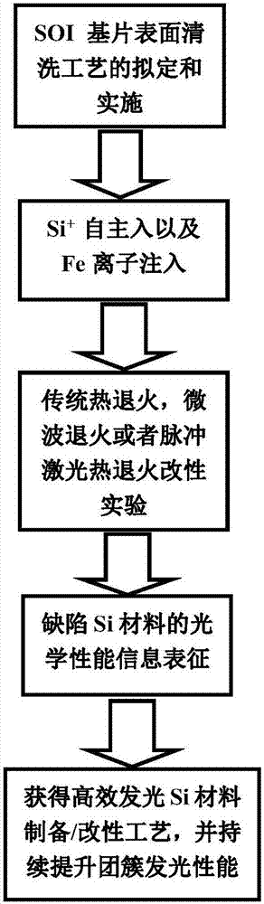
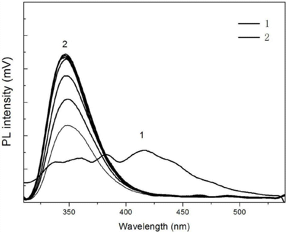
[0018] The method described in this example to introduce auxiliary ions to the modified Si film to improve the optical performance specifically includes the following steps:

[0019] (1) Select the SOI sheet of the P-type Si film with the top crystal orientation of (100), and clean it with the RCA standard cleaning method;

[0020] (2) Using an ion implanter to inject Si + Ions are implanted into the SOI silicon film layer, the incident direction of the ion is 7° to the normal line of the SOI silicon film surface, and it is carried out in a vacuum room temperature environment, Si + The ion implantation dose is 2×10 17 cm -2 , the injection energy is 70keV;

[0021] (3) Si + After the ion implantation is completed, iron ions are implanted into this layer, and the implantation dose is 1×10 15 cm -2 , the injection energy is 70keV. The ion incident direction is 7° from the normal line of the SOI silicon film surface, and the ion implantation process is carried out in a vac...

Embodiment 2

[0024] Step (1), step (2), and step (4) are the same as in Example 1;

[0025] The difference in step (3) is:

[0026] Si + After the ion implantation is completed, iron ions are implanted into this layer, and the implantation dose is 5×10 15 cm -2 , the injection energy is 70keV.

Embodiment 3

[0028] Step (1), step (2), and step (4) are the same as in Example 1;

[0029] The difference in step (3) is:

[0030] Si + After the ion implantation is completed, cobalt ions are implanted into this layer, and the implantation dose is 1×10 15 cm -2 , the injection energy is 70keV.


PUM

PropertyMeasurementUnit
thicknessaaaaaaaaaa
electrical resistivityaaaaaaaaaa
thicknessaaaaaaaaaa

Abstract

The present invention provides a method for improving optical performance by introducing auxiliary ions into a modified Si thin film and belongs to the semiconductor material light emission technical field. According to the method, based on a Si ion self-injecting technique and a rapid thermal annealing process, light emission defects or clusters are generated in a Si film on an SOI substrate. At first, a metal vapor vacuum arc ion source ion injecting machine is adopted to perform ion injection, Si ions and auxiliary ions are injected into an SOI sheet, the top layer of the SOI sheet is (100) crystal orientation P-type single-crystal Si with a thickness of 200 nm, the middle layer of the SOI sheet is SiO2 with a thickness of 375 nm, and the bottom layer of the SOI sheet is P-type single-crystal Si with a thickness of 6.75 microns; and a rapid annealing furnace is adopted to perform rapid annealing on the SOI sheet. The compound injection dose, energy and heating processing process of the auxiliary ions are adjusted, so that the auxiliary ions can be bonded with gap Si atoms, and therefore, exciton fluorescence inactivation energy on an intermediate band can be enhanced. With the method provided by the technical schemes of the invention adopted, the improvement of cluster light emission stability can be facilitated, and therefore, the optical performance of the SOI material can be improved. The method can be popularized in the near room-temperature SOI-LED device field in the aspect of semiconductor light emission materials.

Description

technical field [0001] The invention relates to a method for improving optical properties by introducing auxiliary ions into a modified Si thin film, in particular adopting ion implantation technology and rapid annealing technology to prepare silicon-based luminescent materials, belonging to the technical field of semiconductor material luminescence. Background technique [0002] In recent years, the combination of microelectronics and optoelectronics to develop silicon-based large-scale optoelectronic integration technology has become the inevitable development of information technology and the general consensus of the industry. Silicon is the best candidate material for optoelectronics-microelectronics integration engineering. Compared with other optoelectronic materials, silicon-based optoelectronic materials not only have the characteristics of easy compatibility and integration, but also have the advantages of low cost, high reliability and strong functional expansion; ...

Claims


Application Information

Patent Timeline
Patent Type & Authority Applications(China)
IPC IPC(8): H01L21/265H01L21/324H01L21/02
CPCH01L21/02656H01L21/26506H01L21/324
Inventor 王茺冯晓旭王荣飞李东阳杨杰杨宇刘静
Owner YUNNAN UNIV
Why Eureka
Try Eureka