Composite coating bone pin and preparing method thereof
A composite coating and spicule technology, applied in coating, metal material coating process, superimposed layer plating, etc., can solve the problem of patients suffering from bacterial infection
- Summary
- Abstract
- Description
- Claims
- Application Information
AI Technical Summary
Problems solved by technology
Method used
Image
Examples
preparation example Construction
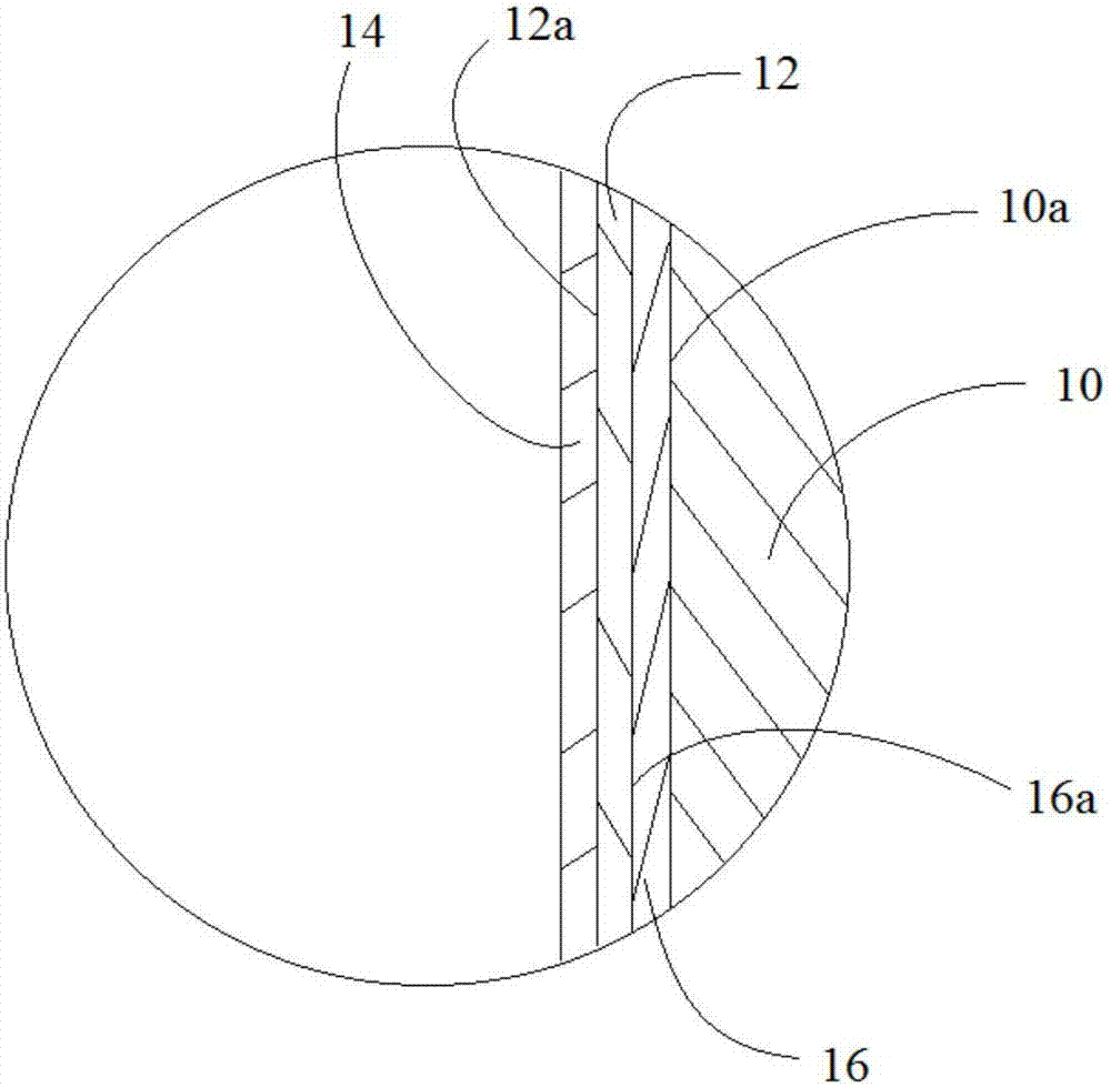
[0021] figure 1 The method for preparing the composite coated spicule 100 according to an embodiment of the present invention includes the following steps:
[0022] Providing a bone spicule 10; performing ion nitriding treatment on the bone spicule 10 to form a nitrided layer 16 on the surface 10a of the bone spicule 10;
[0023] A PVD process is used to deposit a nano hard coating including AlCrN, CrAlN, CrN, TiN, AlTiN, TiAlN, TiAlCrN, TiSiN, TiSiAlN, TiAlWN or a mixture thereof on the surface 16a of the nitriding layer 16 to form the PVD coating 12; and
[0024] The antibacterial nanoparticles are introduced into the PVD process furnace, and the PVD coating 14 modified with antibacterial nanoparticles is formed on the surface 12a of the PVD coating 12 by using the PVD process.
[0025] In an embodiment of the present invention, the antibacterial nanoparticles in the PVD coating 14 modified by antibacterial nanoparticles include silver nanoparticles, copper nanoparticles or a mixture...
Embodiment 1
[0033] Provide a bone spicule; perform ion nitriding treatment on the bone spicule 10 in a nitrogen environment at 400° C. to form a nitriding layer 16 on the surface 10a of the bone spicule 10, with a thickness of 0.25 mm;
[0034] Pass in argon with a purity of 99.999% (ie, high-purity argon), and clean the surface 16a of the nitriding layer 16 under the condition of a bias voltage of 800-1000V; then stop passing argon with a purity of 99.999% Nitrogen (ie high-purity nitrogen), under the conditions of a bias voltage of 80-100V, turn on the Ti target, the arc current is 120A-200A, the surface 16a of the nitrided layer 16 after cleaning is deposited using the PVD process to form a thickness of TiN alloy 3-6μm PVD coating;
[0035] Then, continue to pass in nitrogen with a purity of 99.999% (that is, high-purity nitrogen), keep the CrAl target open under the condition of a bias voltage of 80-100V, and at the same time introduce 1-100nm silver nanoparticles with an arc current of 12...
Embodiment 2
[0037] Provide a bone spicule; perform ion nitriding treatment on the bone spicule 10 in a nitrogen environment at 400°C to form a nitriding layer 16 on the surface 10a of the bone spicule 10, and the thickness of the nitriding layer is 0.3 mm;
[0038] Pass in argon with a purity of 99.999% (ie, high-purity argon), and clean the surface 16a of the nitriding layer 16 under the condition of a bias voltage of 800-1000V; then stop passing argon with a purity of 99.999% Nitrogen (ie high-purity nitrogen), under the conditions of a bias voltage of 80-100V, turn on the Ti target, the arc current is 120A-200A, the surface 16a of the nitrided layer 16 after cleaning is deposited using the PVD process to form a thickness of TiN alloy 3-6μm PVD coating;
[0039] Then, continue to pass in nitrogen with a purity of 99.999% (that is, high-purity nitrogen), keep the CrAl target open under the condition of a bias voltage of 80-100V, and at the same time introduce copper nanoparticles of 1-100nm w...
PUM
| Property | Measurement | Unit |
|---|---|---|
| particle diameter | aaaaa | aaaaa |
| thickness | aaaaa | aaaaa |
| thickness | aaaaa | aaaaa |
Abstract
Description
Claims
Application Information


