Semiconductor structure and formation method therefor

A semiconductor and gate structure technology, which is applied in the field of semiconductor structure and its formation, can solve the problems of low quality gate dielectric layer, affecting transistor performance, and reducing the yield of semiconductor devices, so as to reduce the probability of reaction forming holes and improve Quality and the effect of improving manufacturing yield

Active Publication Date: 2017-07-14
SEMICON MFG INT (SHANGHAI) CORP +1
View PDF6 Cites 0 Cited by
  • Summary
  • Abstract
  • Description
  • Claims
  • Application Information

AI Technical Summary

Problems solved by technology

However, the quality of the gate dielectric layer formed by the prior art is not high, which affect

Method used


Image

  • Semiconductor structure and formation method therefor
  • Semiconductor structure and formation method therefor
  • Semiconductor structure and formation method therefor

Examples


Embodiment Construction

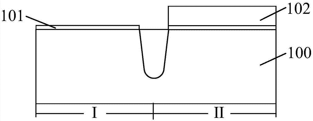
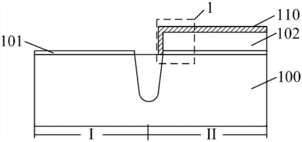
[0038] In the conventional methods for forming semiconductor structures, polysilicon is usually used to form the gate layer, and silicon atoms in the polysilicon are arranged according to certain rules to form crystal grains, and grain boundaries between crystal grains with the same structure but different orientations are easy to form. The grain boundary structure is loose, which is the channel for the rapid diffusion of atoms. During the ashing process, the polysilicon at the grain boundaries is easily oxidized to form silicon oxide. In the subsequent cleaning process, the cleaning agent is easy to react with the silicon oxide at the grain boundary to expand the grain boundary. Therefore, the cleaning agent easily reaches the gate dielectric layer under the gate layer through the enlarged grain boundary, and reacts with the gate dielectric layer to form holes, which reduces the quality of the gate dielectric layer, and then makes the formed semiconductor device invalid.

[...


PUM

PropertyMeasurementUnit
Thicknessaaaaaaaaaa
Thicknessaaaaaaaaaa
Thicknessaaaaaaaaaa

Abstract

The invention provides a semiconductor structure and a formation method therefor. The formation method comprises the steps of providing a substrate; forming a gate dielectric layer on the substrate; forming a gate layer on the gate dielectric layer; forming an amorphous layer for covering the gate layer; and performing patterning on the gate layer and the amorphous layer to form a gate structure. According to the formation method, by performing non-crystallizing on the gate layer, the amorphous layer is formed; the amorphous layer is non-crystals and atoms in the non-crystals are in unordered arrangement, so that a crystal boundary does not exist; and therefore, a cleaning agent which penetrates through the gate layer to arrive at the gate dielectric layer can be reduced in a subsequent cleaning process, thereby lowering probability of hole generation in the gate dielectric layer.

Description

technical field [0001] The invention relates to the technical field of semiconductor manufacturing, in particular to a semiconductor structure and a forming method thereof. Background technique [0002] With the continuous improvement of semiconductor manufacturing technology, semiconductor devices are developing towards higher component density and higher integration. The improvement of semiconductor integration has also led to the reduction of transistor size. [0003] The semiconductor substrate, the gate layer and the gate dielectric layer under the gate layer are the basic components of the transistor. The gate dielectric layer plays an important role in the transistor, which can realize the electrical insulation between the gate and the channel of the transistor, and make the gate and the channel of the transistor form a capacitive structure, so that the control of the gate to the channel current can be realized. [0004] As the size of the transistor decreases, the ...

Claims


Application Information

Patent Timeline
IPC IPC(8): H01L21/28H01L29/423H01L27/115H01L27/11517
CPCH01L29/423H01L29/42324H01L21/28H10B41/00H10B69/00
Inventor 高长城陈其道张京晶
Owner SEMICON MFG INT (SHANGHAI) CORP
Why Eureka
Try Eureka