Production method of InP-based heterojunction bipolar transistor

A heterojunction bipolar and transistor technology, applied in semiconductor/solid-state device manufacturing, semiconductor devices, electrical components, etc., can solve problems such as device function degradation, HBT structure failure, etc., to improve device performance, avoid chemical corrosion, and ensure The effect of electrical properties

Active Publication Date: 2017-07-14
INST OF MICROELECTRONICS CHINESE ACAD OF SCI
View PDF3 Cites 0 Cited by
  • Summary
  • Abstract
  • Description
  • Claims
  • Application Information

AI Technical Summary

Problems solved by technology

[0005] The commonly used photolithography process uses photoresist and developer in the ultraviolet band. The developer in the ultraviolet band is generally alkaline, and the alkaline developer will corrode the GaAsSb epitaxial layer, resulting in greatly reduced device functions and even failure of the HBT structure.

Method used


Image

  • Production method of InP-based heterojunction bipolar transistor
  • Production method of InP-based heterojunction bipolar transistor
  • Production method of InP-based heterojunction bipolar transistor

Examples


Embodiment Construction

[0054] In order to make the purpose, technical solutions and advantages of the embodiments of the present invention clearer, the technical solutions in the embodiments of the present invention will be clearly and completely described below in conjunction with the drawings in the embodiments of the present invention. Obviously, the described embodiments It is only some embodiments of the present invention, but not all embodiments. Based on the embodiments of the present invention, all other embodiments obtained by persons of ordinary skill in the art without making creative efforts belong to the protection scope of the present invention.

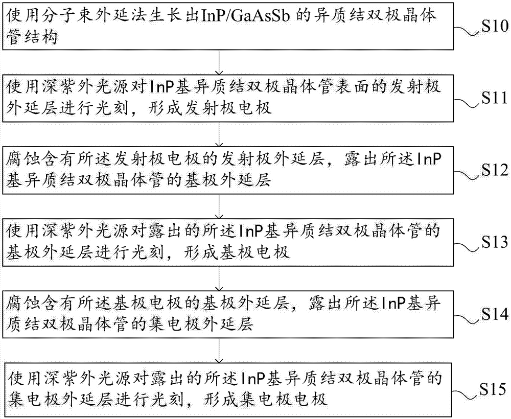
[0055] The invention provides a method for manufacturing an InP-based heterojunction bipolar transistor, such as figure 1 As shown, the method includes:

[0056] S10 , grow an InP / GaAsSb heterojunction bipolar transistor structure by molecular beam epitaxy.

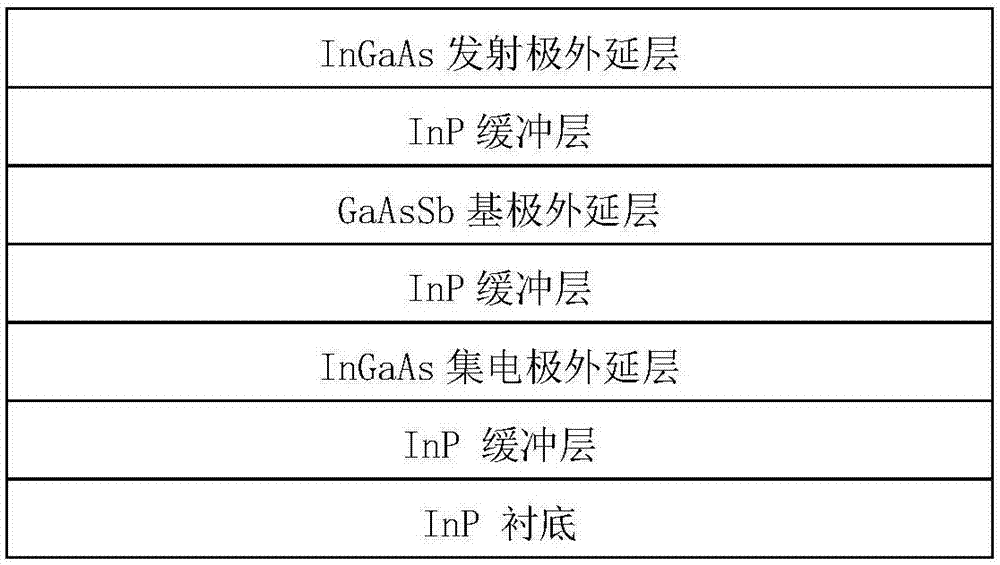
[0057] Specifically, such as figure 2 As shown, the InP / GaAsSb heterojunction bi...


PUM


Abstract

The invention provides a production method of an InP-based heterojunction bipolar transistor. The method comprises the steps of: carrying out photoetching on an emitter epitaxial layer on the surface of the InP-based heterojunction bipolar transistor by using a deep ultraviolet light source so as to form an emitter electrode; corroding the emitter epitaxial layer with the emitter electrode, and exposing a base epitaxial layer of the InP-based heterojunction bipolar transistor; carrying out photoetching on the exposed base epitaxial layer by using the deep ultraviolet light source so as to form a base electrode; corroding the base epitaxial layer with the base electrode, and exposing a collector epitaxial layer of the InP-based heterojunction bipolar transistor; and carrying out photoetching on the exposed collector epitaxial layer by using the deep ultraviolet light source so as to form a collector electrode. According to the production method provided by the invention, PMMA (polymethyl methacrylate) photoresist is used for being matched with deep ultraviolet light to carry out photoetching, and use of an alkaline reagent is avoided, so that chemical corrosion of an alkali substance to GaAsSb is effectively avoided, electric properties of a conducting channel and two-dimensional electron gas are ensured to the greatest extent, and device performance of the InP-based GaAsSb HBT (Heterojunction Bipolar Transistor) is promoted.

Description

technical field [0001] The invention relates to the technical field of semiconductors, in particular to a method for manufacturing an InP-based heterojunction bipolar transistor. Background technique [0002] With the continuous application of high technology in the military field, the frequency of radio frequency and microwave signals is getting higher and higher, the frequency band is getting wider and wider, and the processing capability of digital chips is getting stronger and stronger. Modern warfare has gradually entered the information age and digital age. The rapid development of electronic devices makes the transmission rate of signals faster and faster. With its excellent frequency characteristics, semiconductor devices of III-V compounds have become the modernization of military communications, radar, guidance, space defense, high-speed intelligent weapons and electronic countermeasures. One of the core components of national defense equipment. Especially in the ...

Claims


Application Information

Patent Timeline
Patent Type & Authority Applications(China)
IPC IPC(8): H01L29/737H01L21/331H01L21/027
CPCH01L21/0274H01L29/66318H01L29/737
Inventor 汪宁
Owner INST OF MICROELECTRONICS CHINESE ACAD OF SCI
Why Eureka
Try Eureka