Artificial synaptic device based on photoelectric coupling memristor and modulation method of artificial synapse device

A technology of synaptic devices and photoelectric coupling, applied in the field of artificial neural networks, can solve the problems of restricting the control range and control accuracy of a single synaptic device, limiting the cross-connection of neural synaptic devices, etc.

Active Publication Date: 2017-07-25
HUAZHONG UNIV OF SCI & TECH
View PDF3 Cites 39 Cited by
  • Summary
  • Abstract
  • Description
  • Claims
  • Application Information

AI Technical Summary

Problems solved by technology

At present, the research on artificial synaptic devices is focused on two-terminal synaptic devices; this not only restricts the regulation range and regu

Method used


Image

  • Artificial synaptic device based on photoelectric coupling memristor and modulation method of artificial synapse device
  • Artificial synaptic device based on photoelectric coupling memristor and modulation method of artificial synapse device
  • Artificial synaptic device based on photoelectric coupling memristor and modulation method of artificial synapse device

Examples


Embodiment Construction

[0054] In order to make the object, technical solution and advantages of the present invention clearer, the present invention will be further described in detail below in conjunction with the accompanying drawings and embodiments. It should be understood that the specific embodiments described here are only used to explain the present invention, not to limit the present invention. In addition, each of the present invention described below

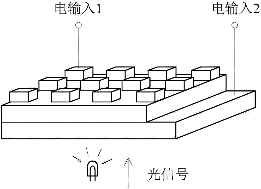
[0055] When electrical signals are only applied to electrical input 1 and electrical input 2, the artificial synapse device can be developed. The technical features involved in the implementation mode can be combined with each other as long as there is no conflict between them.

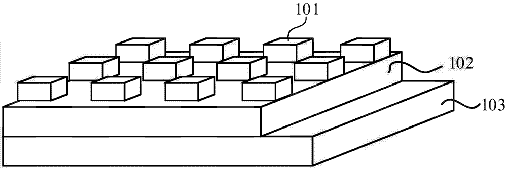
[0056] figure 1 As shown, it is a schematic structural diagram of an artificial synapse device based on an optocoupler memristor provided in the embodiment, specifically including an upper electrode 101, a lower electrode 103, and a functional material layer 102 b...


PUM


Abstract

The invention discloses an artificial synaptic device based on a photoelectric coupling memristor and a modulation method of the artificial synaptic device. The artificial synaptic device comprises an upper electrode, a lower electrode and a functional material layer, wherein the functional material layer is arranged between the upper electrode and the lower electrode, the upper electrode, the functional material layer and the lower electrode jointly form a sandwich structure, the functional material layer is made of a material having a photoelectric effect, the lower electrode is a transparent conductive electrode, an electrical signal is input through the upper electrode and the lower electrode, and an optical signal is input through the transparent conductive electrode. In the artificial synaptic device provided by the invention, light is introduced as a control signal of the other end except the electrical signal, two control ends of the artificial synapse device are expanded to three ends, the artificial synaptic device can generate resistance change under an external optical excitation signal by the additionally-arranged end, the artificial synaptic device can be configured to be in a plurality of resistance states correspondingly by selection and control of intensity, frequency and optical pulse time of the optical excitation signal, and various synaptic plasticity functions are correspondingly achieved.

Description

technical field [0001] The invention belongs to the technical field of artificial neural networks, and more specifically relates to an artificial synapse device based on a photoelectric coupling memristor and a modulation method thereof. Background technique [0002] The existing Von Neumann computer architecture separates data storage and calculation, and data transmission is performed between the memory and the processor through the transmission bus, and its transmission speed will greatly limit the speed of the computer. In the era of big data, the large-scale parallel computing of massive real-time data brings challenges to the existing computing architecture. In the human brain nervous system, computation and storage can be performed simultaneously. Therefore, the research on brain-like computing is expected to become the most effective solution to break through the von Neumann bottleneck. In the human brain nervous system, information processing and storage units are...

Claims


Application Information

Patent Timeline
IPC IPC(8): H01L45/00
CPCH10N70/253H10N70/257H10N70/881
Inventor 李祎段念陈佳周亚雄缪向水
Owner HUAZHONG UNIV OF SCI & TECH
Why Eureka
Try Eureka