
Optical module conversion device based on modulator multichannel demultiplexing

A modulator and multi-channel technology, applied in the field of optical information processing, can solve the problems of limiting sampling rate, application limitation, increasing system complexity, etc., and meet the requirements of increasing sampling rate, easy reconstruction, and reducing bandwidth and sampling rate Effect

Active Publication Date: 2017-07-28
SHANGHAI JIAO TONG UNIV
View PDF5 Cites 23 Cited by
  • Summary
  • Abstract
  • Description
  • Claims
  • Application Information

AI Technical Summary

Problems solved by technology

The sampling rate of PADC based on time division multiplexing is limited by the optical switch speed and the accuracy of optical time synchronization required in the demultiplexing process, so its application is limited
The demultiplexing process based on wavelength division multiplexing technology is very simple, but the number of available channels is limited by the bandwidth of optical devices such as the repetition frequency of the pulsed laser source and the available spectral width, which limits the increase in sampling rate.
[0004] With the continuous improvement of the sampling rate, the optical analog-to-digital conversion technology based on wavelength division multiplexing requires more channels, which increases the complexity of the system

Method used


Image

  • Optical module conversion device based on modulator multichannel demultiplexing
  • Optical module conversion device based on modulator multichannel demultiplexing
  • Optical module conversion device based on modulator multichannel demultiplexing

Examples


Embodiment Construction

[0028] The technical solutions of the present invention will be described in detail below in conjunction with the accompanying drawings and examples, and detailed implementation methods and processes will be given, but the scope of protection of the present invention is not limited to the following examples.

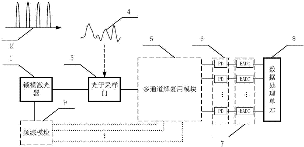
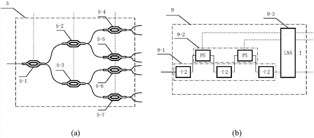
[0029] see figure 1 , figure 1It is an overall architecture diagram of an embodiment of an optical analog-to-digital conversion device based on multi-channel demultiplexing of modulators in the present invention. It can be seen from the figure that the optical analog-to-digital conversion device based on multi-channel demultiplexing of modulators in the present invention is characterized in that it includes high Rate pulse laser 1, photon sampling gate 3, multi-channel demultiplexing module 5, parallel photoelectric conversion module 6, parallel electrical sampling module 7, data processing unit 8 and radio frequency synthesis module 9, the high rate pulse laser 1 is us...


PUM


Abstract

An optical module conversion device based on modulator multichannel demultiplexing comprises a high-rate pulsed laser, a photon sampling gate, a multichannel demultiplexing module, a radio frequency frequency-synthesizing module, a parallelized photoelectric conversion module, a parallelized electrical sampling module and a data processing unit. The multi-channel demultiplexing is realized by using the optical switch effect of the modulator, and the high-speed optical sampling pulse is demultiplexed by the cascading modulator step by step. Finally, the parallelized photoelectric conversion, electrical sampling and data processing are utilized in a compound mode to realize the acquisition of the sampled signal. The device plays a critical role in improving the performance of microwave photon systems which require high sampling rate, high time precision and high sampling precision, wherein the microwave photonic systems comprise microwave photon radars, optical communication systems and the like.

Description

technical field [0001] The invention relates to optical information processing technology, in particular to an optical analog-to-digital conversion device based on modulator multi-channel demultiplexing. Background technique [0002] Signals in nature exist in continuous form, that is, analog signals. In order to facilitate signal transmission, processing and storage, analog signals need to be converted into digital signals. Therefore, the analog-to-digital converter is a bridge connecting the analog world and the digital world. In recent years, electrical analog-to-digital conversion (EADC) technology has developed rapidly. The highest sampling rate of commercial chips in the world is about 30Gs / s, 5.5bit, and the analog bandwidth that the corresponding equipment can handle can reach 30GHz. However, these indicators are close to the theoretical limit of electricity, and further improvement faces great challenges. This is because the design, manufacture and packaging of EADC...

Claims


Application Information

Patent Timeline
IPC IPC(8): G02F7/00H04J14/02
CPCG02F7/00H04J14/0202
Inventor 邹卫文于磊杨光陈建平
Owner SHANGHAI JIAO TONG UNIV
Learn More