Thick film substrate having low void content and high reliability and manufacturing method thereof

A manufacturing method and reliable technology, applied in semiconductor/solid-state device manufacturing, printing devices, printing, etc., to achieve the effect of reducing void rate, ensuring effective welding area, and simple and effective implementation

Active Publication Date: 2017-08-11
NO 24 RES INST OF CETC
View PDF5 Cites 4 Cited by
  • Summary
  • Abstract
  • Description
  • Claims
  • Application Information

AI Technical Summary

Problems solved by technology

[0006] In view of this, on the basis of the grid-like wiring manufacturing process on the back of the conventional thick-film substrate, the present invention solves the inherent problems of the grid-like wiring by improving the wiring method on the back of the substrate, and reduces the thickness on the basis of ensuring the reliability of the substrate. The void rate of the film hybrid circuit after it is put into the shell, therefore, a thick film substrate with low void rate and high reliability and its manufacturing method are provided

Method used


Image

  • Thick film substrate having low void content and high reliability and manufacturing method thereof
  • Thick film substrate having low void content and high reliability and manufacturing method thereof
  • Thick film substrate having low void content and high reliability and manufacturing method thereof

Examples


Embodiment 1

[0037] Fabrication of a Thick Film Substrate with Low Voiding Rate and High Reliability

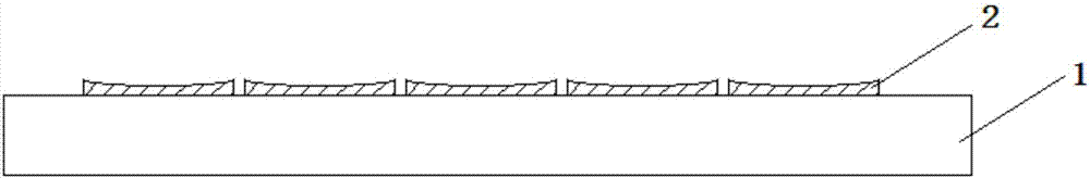
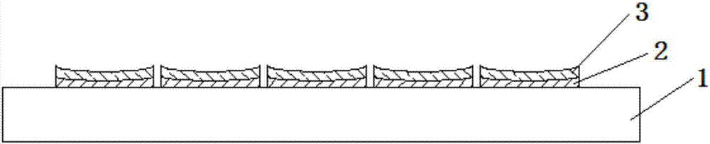
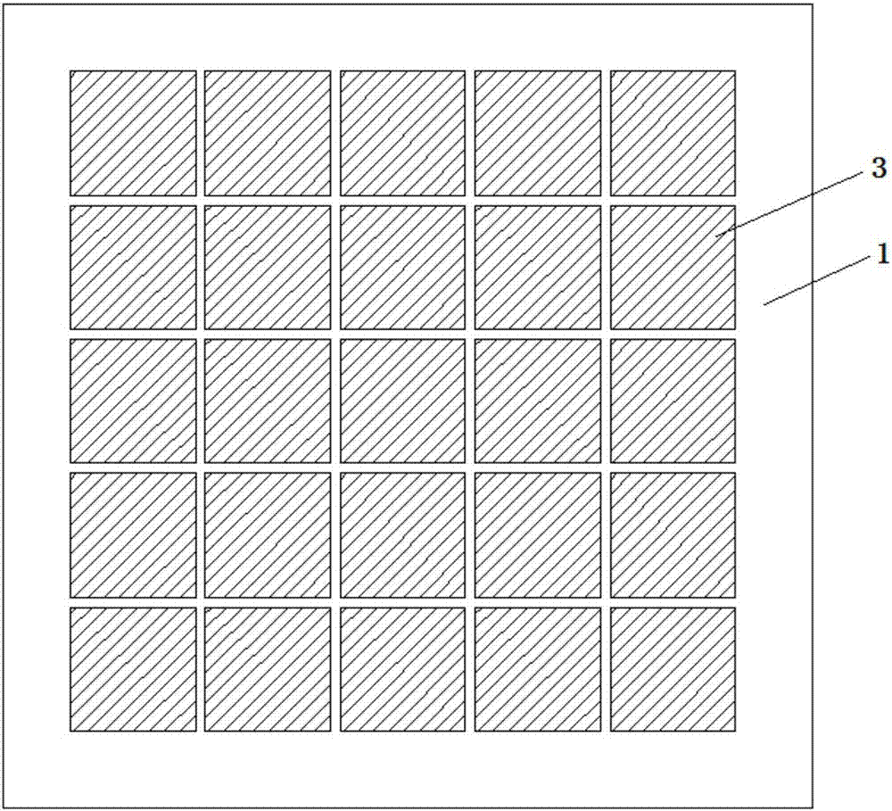
[0038] (1) Use 250-mesh screen to stretch the printing screen frame with a tension of 20N. After cleaning the stretched printing screen frame, stick a 50μm film, dry it at 45°C for 15min, and then use the first grid layer The exposure of the mask plate needs to print graphics. The grid unit size of the printed graphics is 1.85mm×1.85mm, and the gap between the grids is 0.15mm. After the exposure is completed, take out the printing screen frame and remove the mask. After stencil printing, put the printing screen frame into the screen cleaning machine, soak it in warm water at 40°C for 20 minutes, and then rinse and develop it. After the graphic development is complete, seal the area of ​​the screen frame that does not need to be printed with a sealant, and dry it at 45°C 15min, make the required printing screen frame of grid layer;

[0039](2) Use 250-mesh screen to stretch the printing s...

Embodiment 2

[0046] Fabrication of a Thick Film Substrate with Low Voiding Rate and High Reliability

[0047] (1) Stretch the printing screen frame with 250-mesh screen, the tension is 25N, clean the stretched printing screen frame, paste it with 50μm film, dry it at 35°C for 20min, and then use the first grid layer The exposure of the mask plate needs to print graphics. The grid unit size of the printed graphics is 1.85mm×1.85mm, and the gap between the grids is 0.15mm. After the exposure is completed, take out the printing screen frame and remove the mask. After stencil printing, put the printing screen frame into the screen cleaning machine, soak it in warm water at 35°C for 30 minutes, and then rinse and develop it. After the graphic development is complete, seal the area of ​​the screen frame that does not need to be printed with a sealant, and dry it at 35°C 20min, make the required printing screen frame of grid layer;

[0048] (2) Use 250-mesh screen to stretch the printing screen ...

Embodiment 3

[0055] Fabrication of a Thick Film Substrate with Low Voiding Rate and High Reliability

[0056] (1) Use 250-mesh screen to stretch the printing screen frame with a tension of 35N. After cleaning the stretched printing screen frame, stick a 50μm film, dry it at 40°C for 18 minutes, and then use the first grid layer The exposure of the mask plate needs to print graphics. The grid unit size of the printed graphics is 1.85mm×1.85mm, and the gap between the grids is 0.15mm. After the exposure is completed, take out the printing screen frame and remove the mask. After stencil printing, put the printing screen frame into the screen cleaning machine, soak it in warm water at 45°C for 10 minutes, then rinse and develop it. After the graphic development is complete, seal the area of ​​the screen frame that does not need to be printed with sealing glue, and dry it at 40°C 18min, make the required printing screen frame of grid layer;

[0057] (2) Use 250-mesh screen to stretch the print...


PUM

PropertyMeasurementUnit
diameteraaaaaaaaaa
thicknessaaaaaaaaaa
thicknessaaaaaaaaaa

Abstract

The invention relates to a thick film substrate having low void content and high reliability and a manufacturing method thereof. The thick film substrate comprises a ceramic substrate, a first grid layer arranged on the ceramic substrate, a second grid layer arranged on the first grid layer and an emboss layer arranged on the second grid layer, wherein each emboss in the emboss layer is located in the center of each grid of the second grid layer. The emboss layer can effectively reduce the void content of a circuit and improve the heat dissipation of the substrate; meanwhile, the structure can be manufactured by adopting high-palladium silver-palladium paste, so that the binding force between the substrate and a tube shell is guaranteed while the low void content is guaranteed, and the mechanical reliability of the substrate is ensured. The method for manufacturing the thick film substrate is simple and effective, does not have special control requirement in the process manufacturing link, can realize manufacturing by three times of printing and burning, and can be used for large-scale production.

Description

technical field [0001] The invention belongs to the technical field of hybrid integrated circuits, and in particular relates to a thick-film substrate with low void ratio and high reliability and a manufacturing method thereof. Background technique [0002] The thick-film substrate is the carrier component of the hybrid integrated circuit. On the one hand, it provides physical support and electrical connection for the various components on the upper layer. On the other hand, it needs to be tightly combined with the lower shell to ensure heat dissipation and mechanical reliability. Under the premise that the thick film substrate material is determined, the heat dissipation of the circuit is mainly determined by the void ratio of the substrate, and the mechanical reliability is mainly determined by the paste selected on the back of the substrate. [0003] At present, silver-palladium paste is the most commonly used rear wiring paste for thick-film substrates, and the different...

Claims


Application Information

Patent Timeline
Patent Type & Authority Applications(China)
IPC IPC(8): H01L23/15H01L23/367H01L23/492H01L21/48B41M1/12
CPCB41M1/12H01L21/4871H01L21/4882H01L23/15H01L23/3672H01L23/492
Inventor 李华伟张颖殷剑东胡立雪
Owner NO 24 RES INST OF CETC
Why Eureka
Try Eureka