Buffer circuit used for LDO
A buffer circuit, input voltage technology, applied in the direction of adjusting electrical variables, control/regulating systems, instruments, etc., can solve the problems of large power consumption, large circuit area, complex circuit structure of buffer amplifiers, etc. consumption reduction effect
- Summary
- Abstract
- Description
- Claims
- Application Information
AI Technical Summary
Problems solved by technology
Method used
Image
Examples
Embodiment Construction
[0010] The present invention is described in detail below in conjunction with accompanying drawing
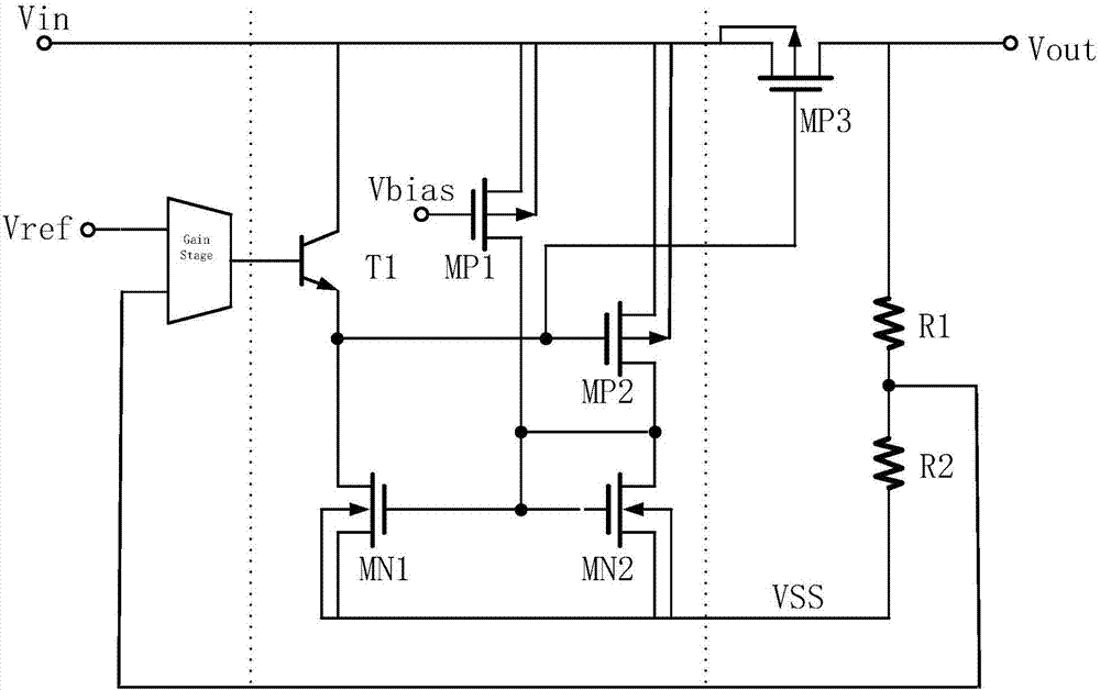
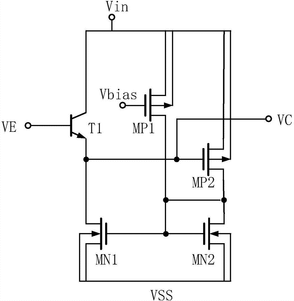
[0011] figure 1 It is the overall circuit block diagram of LDO, which contains the buffer circuit of the present invention. As shown in the figure, the LDO overall circuit includes a reference, an error amplifier, a buffer circuit, an adjustment tube, a feedback loop, and some protection circuits (not shown in the figure). The basic working principle of the entire LDO is to sample the output voltage value through the feedback resistors R1 and R2, and feed back to the error amplifier to compare with the reference voltage. Then the error signal is amplified to drive the adjustment tube to change its resistance to keep the output voltage stable. Compared with the traditional LDO without a buffer circuit, the slew rate of the error amplifier is limited due to the limitation of circuit power consumption. Therefore, when the output fluctuates sharply, the output of the error ampli...
PUM
 Abstract
Description
Claims
Application Information

