Atomic layer etching 3D structures: si and sige and ge smoothness on horizontal and vertical surfaces

An etching and surface modification technology, which is applied in coating, metal material coating process, gaseous chemical plating, etc., can solve the problems of lateral etching material damage and affecting device performance, etc.

Active Publication Date: 2017-08-18
LAM RES CORP
View PDF8 Cites 6 Cited by
  • Summary
  • Abstract
  • Description
  • Claims
  • Application Information

AI Technical Summary

Problems solved by technology

As devices shrink, some techniques used to etch semiconductor materials can cause undesired lateral etching and material damage that can affect device performance and subsequent fabrication processes

Method used


Image

  • Atomic layer etching 3D structures: si and sige and ge smoothness on horizontal and vertical surfaces
  • Atomic layer etching 3D structures: si and sige and ge smoothness on horizontal and vertical surfaces
  • Atomic layer etching 3D structures: si and sige and ge smoothness on horizontal and vertical surfaces

Examples


Embodiment Construction

[0120] In the following description, numerous specific details are set forth in order to provide a thorough understanding of the presented embodiments. The disclosed embodiments may be practiced without some or all of these specific details. In other instances, well known process operations have not been described in detail so as not to unnecessarily obscure the disclosed embodiments. While the disclosed embodiments will be described in conjunction with specific embodiments, it will be understood that it is not intended to limit the disclosed embodiments.

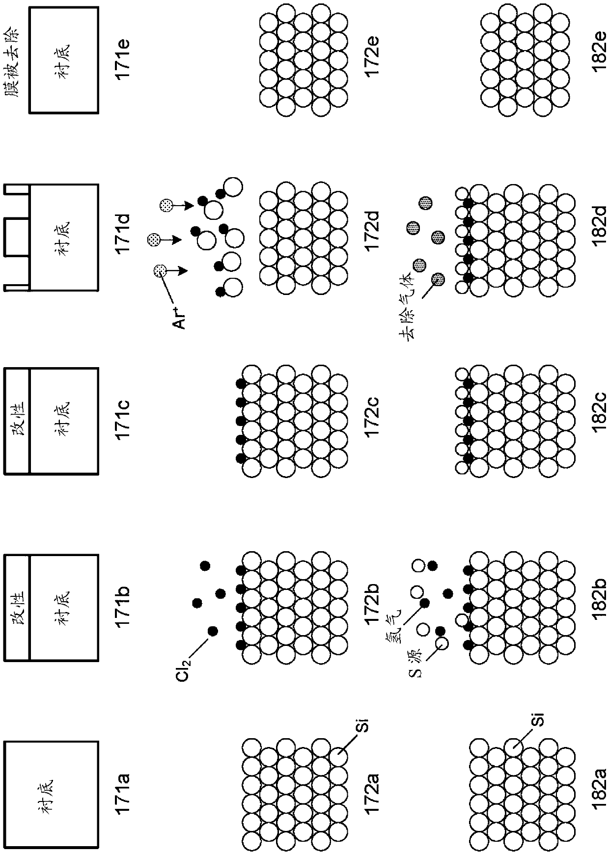
[0121] Semiconductor device fabrication processes generally involve etching processes for forming various structures on semiconductor substrates. Conventional plasma etching processes typically involve continuous etching of materials, but are particularly prone to transport limitations and resulting roughness and damage to etched surfaces. During etching, conventional plasma etching processes combined with pulsing of the ...


PUM


Abstract

The invention relates to atomic layer etching 3D structures: SI and SiGe and Ge smoothing on horizontal and vertical surfaces. Methods and apparatuses for etching semiconductor material on substrates using atomic layer etching by chemisorption, by deposition, or by both chemisorption and deposition mechanisms in combination with oxide passivation are described herein. Methods involving atomic layer etching using a chemisorption mechanism involve exposing the semiconductor material to chlorine to chemisorb chlorine onto the substrate surface and exposing the modified surface to argon to remove the modified surface. Methods involving atomic layer etching using a deposition mechanism involve exposing the semiconductor material to a sulfur-containing gas and hydrogen to deposit and thereby modify the substrate surface and removing the modified surface.

Description

technical field [0001] The present invention relates to the field of semiconductor processing, in particular to methods and apparatus for etching semiconductor materials on substrates using atomic layer etching, and more particularly to atomic layer etching of 3D structures: Si and SiGe and Ge smoothness on horizontal and vertical surfaces. Background technique [0002] Semiconductor fabrication processes typically involve etching semiconductor material with high aspect ratio features. As devices shrink, some techniques used to etch semiconductor materials can cause undesired lateral etching and material damage that can affect device performance and subsequent fabrication processes. Contents of the invention [0003] Methods and apparatus for processing semiconductor substrates are provided herein. One aspect relates to a method of etching a substrate, the method comprising: (a) etching a substrate by performing n cycles of: (i) exposing the substrate to a reactive gas to...

Claims


Application Information

Patent Timeline
IPC IPC(8): H01L21/3065H01L21/67
CPCH01L21/30655H01L21/67069C23C16/45536C23C16/45544H01J37/32009H01J37/321H01J37/32357H01J37/32422H01J37/3244H01J37/32651H01J2237/334H01L21/3065H01L21/70H01L21/02315H01L21/28255H01L21/31116H01L21/32136H01L21/0228
Inventor 萨曼莎·坦杨文兵克伦·雅各布斯·卡纳里克索斯藤·利尔潘阳
Owner LAM RES CORP
Why Eureka
Try Eureka