Capacitance reading circuit and fingerprint recognition system

A technology for fingerprint identification and circuit reading, which is used in the acquisition/organization of fingerprints/palmprints, electronic switches, electrical components, etc. It can solve problems such as reducing the accuracy of fingerprint identification, improve accuracy and efficiency, and eliminate the effect of parasitic capacitance. Effect

Active Publication Date: 2021-03-05
SHENZHEN GOODIX TECH CO LTD
View PDF4 Cites 0 Cited by
  • Summary
  • Abstract
  • Description
  • Claims
  • Application Information

AI Technical Summary

Problems solved by technology

However, there will be a parasitic capacitance between the contact layer and the shielding layer, and the capacitance value of the parasitic capacitance is often greater than the capacitance value of the contact capacitance caused by contact, which affects the capacitance reading circuit or the capacitive fingerprint recognition system to judge the capacitance value of the contact capacitance. As a result, the accuracy of fingerprint recognition is reduced

Method used


Image

  • Capacitance reading circuit and fingerprint recognition system
  • Capacitance reading circuit and fingerprint recognition system
  • Capacitance reading circuit and fingerprint recognition system

Examples


Embodiment Construction

[0029] In order to make the object, technical solution and advantages of the present invention clearer, the present invention will be further described in detail below in conjunction with the accompanying drawings and embodiments. It should be understood that the specific embodiments described here are only used to explain the present invention, not to limit the present invention.

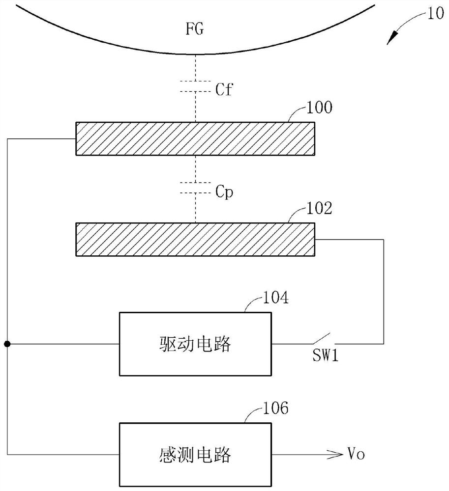
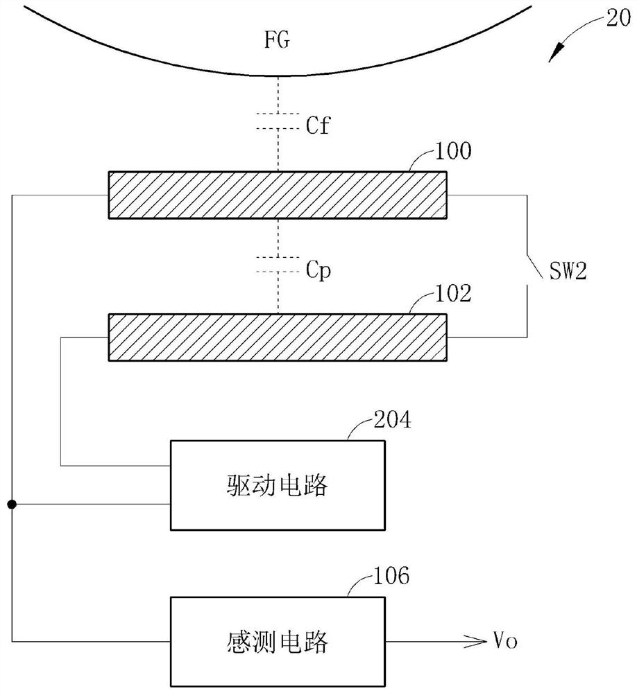
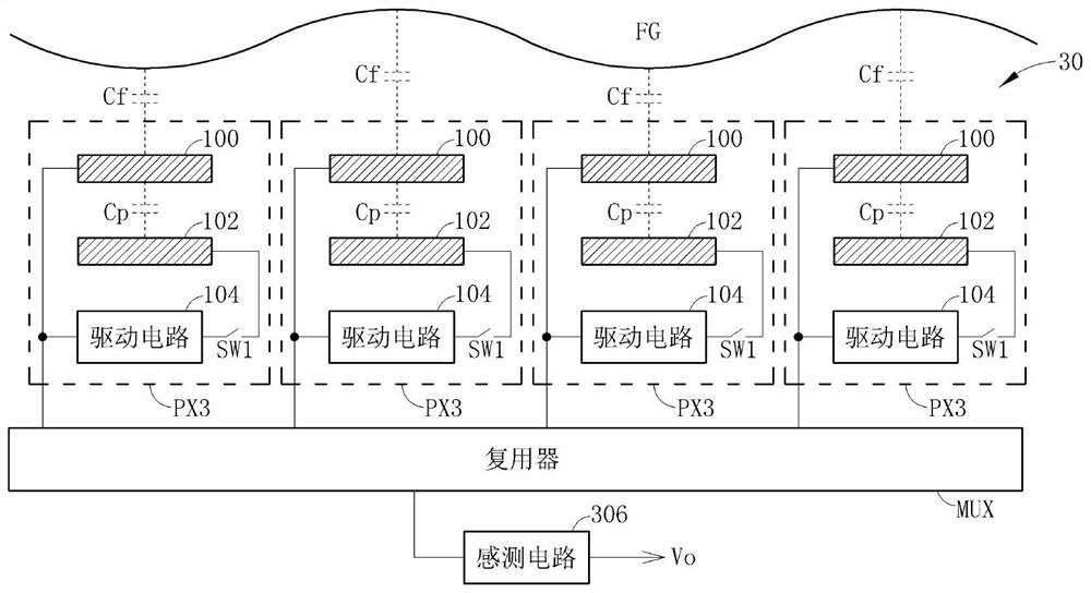
[0030] Please refer to figure 1 , figure 1 It is a schematic diagram of a capacitance reading circuit 10 according to an embodiment of the present invention. Capacitance reading circuit 10 can be applied to a fingerprint recognition system, and is used to judge the capacitance of a contact capacitor, which includes a contact layer 100, a shielding layer 102, a driving circuit 104, a sensing circuit 106 and a switch SW1 (corresponding to first switch). The contact layer 100 can be a top metal layer (Top Metal) of the integrated circuit layout, and is used to receive a contact from a finger FG. Th...


PUM


Abstract

The present invention provides a capacitance reading circuit and a fingerprint identification system. The capacitance reading circuit includes a contact layer for accepting a finger contact; a shielding layer is arranged below the contact layer, and the shielding layer and The contact layer forms a parasitic capacitance; a driving circuit, coupled to the contact layer and the shielding layer; a sensing circuit, electrically connected to the contact layer, used for sensing at a second time the contact capacitor; and a first switch, one end of which is electrically connected to the shielding layer, and the other end is electrically connected to the driving circuit or the contact layer. The capacitance reading circuit and fingerprint identification system provided by the present invention can eliminate the effect of parasitic capacitance, and improve the accuracy and performance of capacitance sensing or fingerprint identification.

Description

technical field [0001] The invention relates to a capacitance reading circuit and a fingerprint identification system, in particular to a capacitance reading circuit and a fingerprint identification system capable of reducing the influence of parasitic capacitance. Background technique [0002] With the rapid development of technology, more and more portable electronic devices such as mobile phones, digital cameras, tablet computers, and notebook computers have become necessary tools in people's lives. Since portable electronic devices are usually used by individuals and have a certain degree of privacy, the data stored in them, such as phonebooks, photos, personal information, etc., are privately owned. Once the electronic device is lost, the data may be used by others to cause unnecessary loss. Although there is currently a password protection method to prevent the electronic device from being used by others, the password is easy to leak or be cracked, and has low securit...

Claims


Application Information

Patent Timeline
Patent Type & Authority Patents(China)
IPC IPC(8): G06K9/00
CPCG06V40/1306G06V40/1329G06F3/0416G06F3/044H03K17/962G06F2203/04107
Inventor 赵国豪杨孟达
Owner SHENZHEN GOODIX TECH CO LTD
Why Eureka
Try Eureka